Hi Guys,
I've got a similar project going on right now. I was trying to foster feedback in another thread but I think this is a more appropriate place. For reference: https://www.diyaudio.com/forums/ana...simple-opamp-preamp-issues-2.html#post5937777
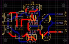
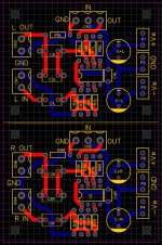
My idea is for a dual mono variant of the P88 with separated grounds for supply rails and signal. It is designed to be modular thats not tied to specific part choices. That and it has spade connections for the supply rails, I love spade connectors. The penalty is increased size: 100mm x 85mm.
Here's my working schematic and first draft of the pcb.
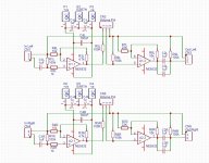
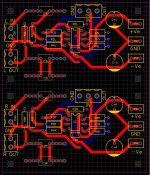
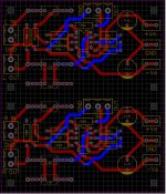


2. Impedances around the opamps in P88 and P06 are decidedly on the high side and IMHO would give higher noise levels than necessary, especially since OPA2134s and NE5532s are rather good load drivers and not easily impressed by loads even down in the low kOhms. Presumably the values were chosen for the much weaker TL072. I would suggest lowering them by about a factor of 3 for starters, maybe up to 5. (In P06, this would be R2-R7, in P88, R3/4+7/8.) The crux: Any capacitors forming RC time constants have to be increased accordingly, with much fewer values available, so if in doubt select Cs first.
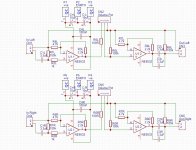
I noticed some inconsistencies on that last schematic and decided to have another look. I also took your advice and lowered the value of the resistors in the feedback network.
Here is the next version. I am also reconsidering the need for large sized resistors on the boards. I'm sure they could be made a bit more compactly with a bit more thought about what is most likely to be on the boards.
Which power supply will you be using?
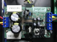
I'm am no expert on a PSU for solid state line stage. The psu I am using right now is almost the same as the one recommended by Rod Elliot. It's a $20 kitset from a local supplier Jaycar.
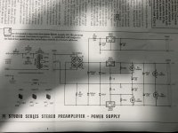
I know I could make something decent with 2x LT1086 along these lines.
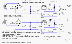 .
. I even have some boards for this schematic due imminently that could be repurposed. The boards are a larger than necessary for the current requirements here.
I am open to more exotic designs. What are your thoughts on the most appropriate PSU?
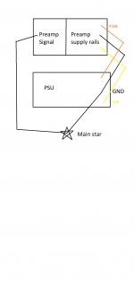
Connected to the PSU star Ground i guess !!!I see no connection between the power ground and the signal ground. I am curious what is the path of the return signal currents?
I thought that after so many discussions on this forum the star ground idea has been successfully retired but as I see now it is still there...
I am curious if you can see a perfect aerial in your sketch? If your intention is to avoid interference then the approach you have chosen leads you in the opposite direction.
I am curious if you can see a perfect aerial in your sketch? If your intention is to avoid interference then the approach you have chosen leads you in the opposite direction.
I thought that after so many discussions on this forum the star ground idea has been successfully retired but as I see now it is still there...
I am curious if you can see a perfect aerial in your sketch? If your intention is to avoid interference then the approach you have chosen leads you in the opposite direction.
Thank you, I think I can see what you are getting at there.
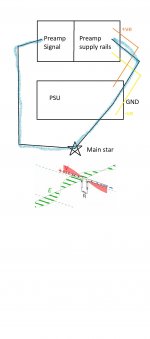
So best practice would be to ground the signal stage 'above' psu like one typically sees in commercial offerings? Signal stage > On board decoupling > PSU > chassis earth.
Last edited:
I can not fully follow your last sentence but the best you can do to your PCB is to flood the bottom of the PCB with the continuous ground plane connecting all grounds, power and signal, and route most if not all other traces on the top layer. I would also add rail to ground ceramic decoupling capacitors near the op-amp power pins for both power rails. A single rail to rail decoupling capacitor may not be enough for some op-amps. I also recommend to use a 3 pin 5mm pin spacing screw terminal for the power entry. It will take less space on the PCB. The IN and OUT pin labels of the CN2 connector are swapped. I would also suggest to avoid making your PCB as a panel of two identical boards since you'll get 10 of them from the manufacturer anyways and if manufacturer sees a panelized design they'll add a premium to the total price of your order for that.
I can not fully follow your last sentence but the best you can do to your PCB is to flood the bottom of the PCB with the continuous ground plane connecting all grounds, power and signal, and route most if not all other traces on the top layer. I would also add rail to ground ceramic decoupling capacitors near the op-amp power pins for both power rails. A single rail to rail decoupling capacitor may not be enough for some op-amps. I also recommend to use a 3 pin 5mm pin spacing screw terminal for the power entry. It will take less space on the PCB. The IN and OUT pin labels of the CN2 connector are swapped. I would also suggest to avoid making your PCB as a panel of two identical boards since you'll get 10 of them from the manufacturer anyways and if manufacturer sees a panelized design they'll add a premium to the total price of your order for that.
I decided to take your advice
In the first usage these boards will be placed near the back of the enclosure. The signal terminals should face the back, the power supply terminal should face the left of the enclosure and the volume pot terminal should face the right side. This should allow me to easily stack 2 boards and route wiring nicely.
I flooded the bottom with the ground plane except one small section for the positive power rail.
I have changed the psu terminals to a 3 pin 5mm pitch screw terminal as spade connectors would make stacking difficult as well as the increased real estate.
I changed the single rail to rail decoupling cap to a pair of rail to ground caps.
I changed the design to a single mono board. I'll have to order 10 instead of 5 which is a marginal extra charge and will save me the bother of separating the halves of a panelised design.
I was also missing the 100R resistor on the output on the previous version.
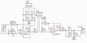
Here's the new schematic and my current PCB design.
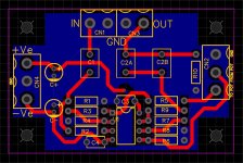
Ah, don't you just love it when you're being given conflicting advice? More so when everyone's actually got a point?
Fact is, you need to reconcile all of it at the end of the day (AF and RF), and there is more than one approach for doing so. Star grounding by the book pays no mind to parasitic inductance and in fact assumes a necessarily non-zero ground return impedance, while the RF guys like to brute force ground everything with groundplanes and low inductance, with parasitic ground resistance being assumed to be "too small to matter". Both extremes can bite you in the rear end.
Let's take a page out of the book of mass market hi-fi manufacturers for an example of how to make things work. They will put everything into a well-connected metal case and use the back panel as their "star ground point", with (cheap) non-insulated RCA jacks galore. This then will keep most of the mean old world out (thank Mr. Faraday), with input RF filtering doing the rest. Any RF potentially coming in via the mains cable has a tendency of not making it past the transformer and snubber capacitors in the power supply. So basically there is no RF to speak of inside the unit, giving you great liberty in star grounding to avoid having your transformer inducing hum into internal connections that are part of ground loops. Remember, we're talking a plain ol' analog preamp. Not a CD player, DVD player or DVR, not even a power amp.
Equipment of the 1970s had some real adventurous grounding schemes going on at times. Like the "bus" type shared power/signal ground running from back panel, phonopre, volume / tone amp up to power amp input, usually on several separate boards connected by cables... a real joy if you need to implement some extra power supply filtering somewhere in between, which with any luck will inject a good amount of power supply noise into the ground.
Now there still are certain things that you can do to keep ground return impedance (resistance and inductance) low:
* Use nice and thick traces (even fills can be good as long as they don't have big holes, again: loops)
* Inductance hinges on loop area, so where you cannot avoid length you may still be able to keep things close together in another dimension (see e.g. twisted V+/V-/GND wiring, which could be taped to the chassis floor to top it off; this is also crucial in power amp layouts in anything not Class A)
* You can use metal standoffs to attach a groundplane to chassis (screws with lock washers recommended), but then I would partition the groundplane into as many sections as you've got standoffs with thin slots, to be bridged only with smallish (like tens of nF max) ceramic caps to make the RF guys happy. And then you still need to get your power ground sorted, which ought to return to the power supply first - if you can afford it, I might give it its very own dedicated groundplane.
You should be a bit careful with groundplanes / fills, as they can be detrimental in some spots where they would introduce extra capacitive coupling to ground, e.g. underneath opamp (-in) pins or feedback components.
Note how a holistic approach is needed ro achieve a near-optimum result.
Last edited:
Version 3.0somethingorother
G'day guys,
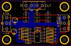
Here's my current version. I had a good stare at my previous arrangement and it was beginning to look problematic with lots of potential for looping. There was also a major error with fill around the input at CN1
I've ended up with something approximating a ground bus arrangement terminating at the ground rail to the PSU.
I'm not certain I am quite there yet. My main concern with this iteration is the 100nf PSU decoupling caps (C3 and C4) being so close to ground side termination of R1 and R4.
How much pollution from the rail decoupling is likely to be introduced to the signal ground in this arrangement? I'm going to follow Rod Elliot here and use 100nf ceramic caps. I'm hoping that there should be minimal noise left by this point to be filtered out. Does anybody have any thoughts here?
Also I have been pondering the PSU side of things a bit more. My thinking right now is to have my own PSU boards fabbed at the same time as I am certain I would have use for the surplus boards later on.
I've decided to go with the dual LT1086 idea as these seem to be the lowest noise of the commonly available regulators from reading the spec sheets.
Here's my working schematic. It is based mostly off the LT1086 spec sheet with the CRC filter pinched from Rod Elliot P05 and some extra 100nf snubbers for the larger electrolytic caps.
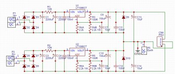
Here's my draft PCB
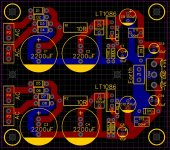
G'day guys,

Here's my current version. I had a good stare at my previous arrangement and it was beginning to look problematic with lots of potential for looping. There was also a major error with fill around the input at CN1
I've ended up with something approximating a ground bus arrangement terminating at the ground rail to the PSU.
I'm not certain I am quite there yet. My main concern with this iteration is the 100nf PSU decoupling caps (C3 and C4) being so close to ground side termination of R1 and R4.
How much pollution from the rail decoupling is likely to be introduced to the signal ground in this arrangement? I'm going to follow Rod Elliot here and use 100nf ceramic caps. I'm hoping that there should be minimal noise left by this point to be filtered out. Does anybody have any thoughts here?
Also I have been pondering the PSU side of things a bit more. My thinking right now is to have my own PSU boards fabbed at the same time as I am certain I would have use for the surplus boards later on.
I've decided to go with the dual LT1086 idea as these seem to be the lowest noise of the commonly available regulators from reading the spec sheets.
Here's my working schematic. It is based mostly off the LT1086 spec sheet with the CRC filter pinched from Rod Elliot P05 and some extra 100nf snubbers for the larger electrolytic caps.

Here's my draft PCB

Last edited:
You should give Elvee's denoiser a go---pretty simple but amazingly effective:I haven’t settled on a psu yet. The existing mark 1 is using a lm337/317 regulated supply @ +/- 15v. I am toying with the idea of making something a bit nicer
D-Noizator: a magic active noise canceller to retrofit & upgrade any 317-based V.Reg.
I'm going to follow Rod Elliot here and use 100nf ceramic caps. I'm hoping that there should be minimal noise left by this point to be filtered out. Does anybody have any thoughts here?
100nF Monolithic 50V X7R. IIRC all the capacitors on the P88 PCB went across the rails and not to ground. I can't remember the section with the 2 electrolytics as I only have the first stage PCB left.
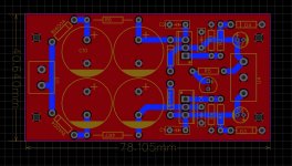
So here's my version of a 317/337 power supply. Very much inspired by the rod elliott / doug self / muffsy designs of course. i'm very new to pcb design so any feedback would be welcome.
Sadface - you mentioned going for a dual LT1086 design for lower noise. What kind of noise figures are you expecting?

Sadface - you mentioned going for a dual LT1086 design for lower noise. What kind of noise figures are you expecting?
- Home
- Source & Line
- Analog Line Level
- Rod Elliot Project 88 question
