Andrew, a schematic is just a node connection diagram. Very rarely does a schematic attempt to show similarity to a preferred layout - the only time I've seen that done is when someone wants to specifically show a star ground node with more than four traces joining at a single node. The closest a schematic comes to layout reality is probably for the old style tinned-copper wire bus that encircled old amps - but that is in the eye of the beholder and is not dictated by the schematic drawing. Imho, SGK's schematic is fine.
If you can see something that could be done better with the layout then that would be good feedback - but to me it looks fine for handling rectifier pulses, given the middle-of-the-road noise application.
If you can see something that could be done better with the layout then that would be good feedback - but to me it looks fine for handling rectifier pulses, given the middle-of-the-road noise application.
Which of those aren't done on the board? Showing the schematic as one would route the board is often impractical. Andrew would have On Semi redraw their data sheet circuit diagrams including Fig 20. The guidance with respect to routing the board is relevant; the demands with respect to the schematic seem to be just argumentative.
From post 19 (numbering added):
1. Done (from beginning)
2. Done (from beginning)
3. Once again, do you object to the use of the 0V plane? [With respect to R2, I sample 12V output at the output connectors.]
4. Done (trobbins suggestion implemented early in post 18)
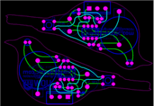
Attempting to load the image referenced in post 40 a different way as I still can't upload to the forum...
From post 19 (numbering added):
- The -ve of the upper bridge connects to the -ve of C1.
- The -ve of the lower bridge connect to the -ve of C5.
- R1 and C3 need to connect. This then connects to the output at C4.
- R3 and C7 need to connect. This then connectss to the output at C8.
1. Done (from beginning)
2. Done (from beginning)
3. Once again, do you object to the use of the 0V plane? [With respect to R2, I sample 12V output at the output connectors.]
4. Done (trobbins suggestion implemented early in post 18)
Attempting to load the image referenced in post 40 a different way as I still can't upload to the forum...
An externally hosted image should be here but it was not working when we last tested it.
Last edited:
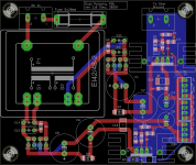
My preliminary investigations today with my Quasimodo jig and a Block PT series 7.5VA 2x15V pcb transformer suggests that leaving the capability for a full CRC snubber makes sense and so I have left these in the design. I also adapted the transformer footprint so as to accommodate both the EI42-2 and the larger EI48-2 footprint transformers. Block make the PT 7.5/2/15 and the VC 10/2/15 in this larger size. I think this is getting close to final.
Attachments
BTW I hope that one of the first uses for this PSU is going to be this little guy:
http://www.diyaudio.com/forums/soli...ow-noise-unity-gain-balanced-input-stage.html
...the most challenging PCB layout I have attempted yet
http://www.diyaudio.com/forums/soli...ow-noise-unity-gain-balanced-input-stage.html
...the most challenging PCB layout I have attempted yet
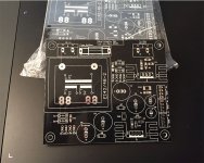
Just arrived...
Yes I ticked black for a bit of a laugh. It matches one of my passports and the kit of my favourite sports team.
I haven't taken a close look at the quality yet. Manufactured by pcbway and had them within 5 days of sending the order.
Yes I ticked black for a bit of a laugh. It matches one of my passports and the kit of my favourite sports team.
I haven't taken a close look at the quality yet. Manufactured by pcbway and had them within 5 days of sending the order.
Attachments
re: Thermal considerations for Fairchild SDIP bridge rectifiers
I suggest you purchase inexpensive equipment such as this which lets you measure the temperature of your bridge rectifiers, safely. With little danger of electric shock. Naturally you should first verify that your measurement machinery gives answers that match known-good thermometers.
When I did this myself, I connected the max rated load, and I found that the diode temperature-vs-time took about 30 minutes to stabilize at a final value that didn't change. The transformer, on the other hand, was a big heavy lump of grain oriented silicon steel and it took more than 2 hours to heat itself up to its final asymptotic temperature.
Thanks Mark. I will pick one up.
FYI I don't like how cramped things were between the E48 size transformer and the heatsink to the right of it when I was making up the first board. (See attached.) Stuff fits, but it is very tight and unnecessarily so as the board was 80x95mm and I had a further 5mm of width available while still staying within the freeware board size constraint of Eagle. Silly. The boards would have cost the same to manufacture also. (And I purchased a Eagle Make Personal license and so no longer face such a tight board dimension constraint.)
So I have done a revised version adding the 5mm of width back and spacing out the diodes a bit more. I still think the first version is technically ok although I have not had the chance to plug it in and test it yet though.
If anyone thinks it worthwhile, I will happily post gerber files for people to use for their own non-commercial purposes (building at your own risk as this involves mains voltages).
Merry Christmas!
Attachments
It is interesting to read that Self suggests using a 47uF capacitor from the LM317 adjust pin (C3 and C7 in the circuit in post 43) rather than the 10uF suggested in the data sheet. A larger cap would take up more space (or require moving from an X7R) although one can get a 22uF X7R MLCC in a moderately sized case code of 1210 imperial.
As I searched I noted the existence of stacked ceramic caps which were typically larger class 1 devices. Have you guys ever just stacked a couple of SMD caps on top of each other, eg soldering two 1210 on top of each other, to double the capacitance in a given SMD footprint? Does this make sense any at all?
(I note also that I really should make this supply +/- 15v if it is used to drive the project linked to in post 45.)
Last edited:
Stacking is certainly fine to do, especially where the pad allows a bit more solder - but is obviously diy.
Adding pads without drilled holes on the non-component side is also very beneficial for mounting SMD parts - especially for bypass caps that effectively minimise the loop area of a switchmode or charging pulse - eg. a cap placed at the diode pads, to bypass the main electrolytic cap. Similarly for adding RC snubbers to windings directly at the transformer pads.
Adding pads without drilled holes on the non-component side is also very beneficial for mounting SMD parts - especially for bypass caps that effectively minimise the loop area of a switchmode or charging pulse - eg. a cap placed at the diode pads, to bypass the main electrolytic cap. Similarly for adding RC snubbers to windings directly at the transformer pads.
Yes using SMD components to implement the snubbers, laid out exactly upon the transformer pads (highly optimized layout on bottom side), enables you to reduce the total length of the current loop from 3.3 inches, to 3.1 inches. Whether this is, or is not, significant, requires further calculations.Similarly for adding RC snubbers to windings directly at the transformer pads.
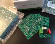
BTW I continue to be very, very impressed with PCBWay.
http://www.pcbway.com
I placed an order for a slightly revised version of this PCB last Thursday. The same day I sent them another PCB which is an output relay board for an amplifier project I am working on.
These were my second and third PCBs from them. The output relay PCB was my first attempt at panellising and requesting a PCB manufacturer to add v-scores to the panel. (I added the following instructions in my order request in the relevant box in the order submission process via their website: V score along both horizontal and vertical lines on top silk. Web = 0.005")
I made a mistake uploading one of the folders of Gerber files and missed the drill file. Erin from customer service/sales sent me an email explaining my mistake and all was solved with a simple reload of the folder via their website. Very good service.
All the boards arrived today - just 4 working days later - via DHL courier. Packaging was excellent and the boards seem to be of very high quality again. All the boards were 2 layer, 1oz copper. Pricing frankly could not be much better. The ten 8x10cm PSU boards cost $13. The ten 8x8cm panels of four 4x4cm output relay boards cost $25, the extra cost because it was a panel. If boards are less than 10x10cm the cost is the same for 5 or 10 boards.
Shipping via DHL was $36 for the combined order and I had to cover Paypal fees of $4 less a $1 credit. (I did have to pay £20 to DHL for VAT and their handling of the VAT payment - so annoying to pay a £10 handling fee to pay £10 in tax to the government. Very efficient.)
Separating the panel was absolutely easy - they easily snapped along the v-score with modest pressure. One could simply leave the snapped PCB as is thereafter but I gave the edges a quick rub with a sanding block.
From my experience I would certainly recommend their service.
PS: if anyone can use an output relay board I have lots spare.
Attachments
Last edited:
heat removal requires a plane underneath for safe thermal
Copper traces ---- the standard 1 ounce of copper per square foot default ----- are easily modeled as 70 degreesC/watt. For any size square of foil
Thus a trace 0.1" wide, but 1 inch long and thus 1/0.1 = 10 squares of foil,
will exhibit 700 7-0-0 "7 hundred" degreeC per watt of heat flow.
(This high resistance is useful when crafting thermally-controlled PCBs for thermocouple sensor interfaces.)
Another approach to heat removal is to dump the heat thru the FR-4 into an underlying plane (power or GND) and let the plane spead out the heat.
We use the same concept: 70 degreeC/watt per square of foil.
And view the FR-4 as 100X worse (that 100X is from my memory) than copper, but the long power trace has many opportunities to dump heat vertically into the underlying plane.
You may model these PCBs as GRIDS of resistors in SPICE. Start with 0.06" grid which is the standard PCB FR-4 insulating thickness. Make the vertical resistors 7,000 ohms. Make the two horizontal resistive layers be 70 ohms.
We'll drive the top layer.
We'll use the bottom layer, grounded (to SPICE node 0) at one end, as the heat-exit path.
Drive the top layer with 1 amp current source and probe how that one amp eventually all transfers thru the host of 7,000 ohm resistors and ends up on the bottom layer.
By the way, you can model silicon substrates in the same manner.
Thanks tankcircuitnoise. I need to spend more time with this.
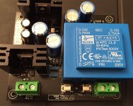
On a different note, one thing that I've thought about recently with respect to this little PSU is that it is potentially unfortunate that the Block VC series transformers I am using have primaries designed for 230V only. Other Block transformers, namely the AVC series, have dual 115V primaries. It would seem sensible for me to consider in future iterations using an AVC series transformer and incorporating a small switch to allow changing between series and parallel configuration of the primaries.
To that end, I'd like to check if there would be any issues (particularly with respect to safety) of using a small DPDT slide switch such as a Grayhill 48ASDP1S1M2QBT (Mouser link) (Datasheet link) for this purpose. It would seem suitably small and is rated for 250VAC and 5A. I check because mains voltages make me safety conscious.
Also, Mark you recommended using STP2L60 diodes (mounted vertically). I was wondering if there was a particular characteristic of these diodes that drove this advice versus, say, using something like a DF06M.
I did a Parametric Search on digikey.com for
It was a delight to see that its datasheet gave an I-V curve, and also quoted a junction-to-ambient thermal resistance for infinitely long leadlength, i.e., not dumping any heat into the copper of the PCB.
Plugging the datasheet numbers into calculations: if you ran these diodes at 500mA apiece, which is a ridiculously conservative overestimate, because (a) when a bridge rectifier supplies X amperes, each diode conducts only X/2 amperes; and (b) your transformer secondaries are only rated for 180mA ... then at 500mA the diode forward voltage drop would be 0.45 volts and the diode power would be 0.225 watts. Multiplying by the thermal resistance, the diode junction temperature would be 23 degrees C higher than the ambient air. This seemed like a very comfortable cushion, a huge safety margin, when suggesting possible components in a discussion thread entitled
Thermal considerations for bridge rectifiers
- Schottky diodes rated 50 volts or higher
- in small thru-hole packages with axial leads: DO-15, DO-41, DO-35, DO-204
- rated for continuous DC current of 1A or greater
It was a delight to see that its datasheet gave an I-V curve, and also quoted a junction-to-ambient thermal resistance for infinitely long leadlength, i.e., not dumping any heat into the copper of the PCB.
Plugging the datasheet numbers into calculations: if you ran these diodes at 500mA apiece, which is a ridiculously conservative overestimate, because (a) when a bridge rectifier supplies X amperes, each diode conducts only X/2 amperes; and (b) your transformer secondaries are only rated for 180mA ... then at 500mA the diode forward voltage drop would be 0.45 volts and the diode power would be 0.225 watts. Multiplying by the thermal resistance, the diode junction temperature would be 23 degrees C higher than the ambient air. This seemed like a very comfortable cushion, a huge safety margin, when suggesting possible components in a discussion thread entitled
Thermal considerations for bridge rectifiers
BTW I continue to be very, very impressed with PCBWay.
China PCB Prototype & Fabrication Manufacturer - PCB Prototype the Easy Way
I placed an order for a slightly revised version of this PCB last Thursday. The same day I sent them another PCB which is an output relay board for an amplifier project I am working on.
These were my second and third PCBs from them. The output relay PCB was my first attempt at panellising and requesting a PCB manufacturer to add v-scores to the panel. (I added the following instructions in my order request in the relevant box in the order submission process via their website: V score along both horizontal and vertical lines on top silk. Web = 0.005")
I made a mistake uploading one of the folders of Gerber files and missed the drill file. Erin from customer service/sales sent me an email explaining my mistake and all was solved with a simple reload of the folder via their website. Very good service.
All the boards arrived today - just 4 working days later - via DHL courier. Packaging was excellent and the boards seem to be of very high quality again. All the boards were 2 layer, 1oz copper. Pricing frankly could not be much better. The ten 8x10cm PSU boards cost $13. The ten 8x8cm panels of four 4x4cm output relay boards cost $25, the extra cost because it was a panel. If boards are less than 10x10cm the cost is the same for 5 or 10 boards.
Shipping via DHL was $36 for the combined order and I had to cover Paypal fees of $4 less a $1 credit. (I did have to pay £20 to DHL for VAT and their handling of the VAT payment - so annoying to pay a £10 handling fee to pay £10 in tax to the government. Very efficient.)
Separating the panel was absolutely easy - they easily snapped along the v-score with modest pressure. One could simply leave the snapped PCB as is thereafter but I gave the edges a quick rub with a sanding block.
From my experience I would certainly recommend their service.
PS: if anyone can use an output relay board I have lots spare.
Very useful experience . Maybe I will try PCBWay later.
- Status
- This old topic is closed. If you want to reopen this topic, contact a moderator using the "Report Post" button.
- Home
- Amplifiers
- Power Supplies
- Thermal considerations for Fairchild SDIP bridge rectifiers