A conceptual question about composite voltage regulators. Looking at the provided schematic, R1 and R2 are user-adjustable (potentiometer) for the desired output voltage. VREF is a precision reference, and the opamp is a precision opamp. The negative feedback loop (if I have drawn it correctly) causes the opamp to adjust the common pin of the 7805 voltage regulator through a transistor, but I guess there are two ways of doing it. My question is: which way is correct?
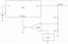
In this first picture, the feedback opamp adjusts the NPN transistor, which in turn adjusts the common pin of the voltage reulator. I guess you could say this is the "current mode" adjustment, because the NPN transistor draws a current from the collector, and the collector output is high impedance.
==> The opamp output voltage controls the voltage regulator "common" pin via a current.
Attachments
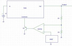
In this second schematic, the transistor is now a PNP, and the opamp terminals have been reversed to preserve negative feedback.
The output opamp voltage is now buffered by the PNP transistor (common collector), which leads to the common pin of the 7805 voltage regulator.
==> The opamp output voltage controls the voltage regulator through the buffered voltage via the PNP transistor.
==> Which method is correct (current or voltage), or leads to better performance?
Attachments
I have to say, if you are in that far you should just replace the 78xx with a proper pass transistor driven by a CCS from which the opamp steals base drive. A real super-regulator.
The problem with the layout illustrated is that, however good your voltage reference and opamp/f/back network, the output will be dominated by the noise and internal error-amp performance of the three pin reg. In other words the composite will allow you higher output voltage, but not necessarily better performance. Sorry!
The problem with the layout illustrated is that, however good your voltage reference and opamp/f/back network, the output will be dominated by the noise and internal error-amp performance of the three pin reg. In other words the composite will allow you higher output voltage, but not necessarily better performance. Sorry!
I simulated something that looked similar, once, mainly to try to eliminate voltage variations due to fluctuations in load current, as well as to try to eliminate any noise or ripple that made it through the regulator. It worked quite well, although it needed a negative supply rail for the opamp. The opamp's positive supply came from the regulator output (So a 7805 might need a low-voltage opamp. I was doing 12v regs, dual supply.).
It was somewhat similar to your second schematic, but with no transistor (i.e. opamp output went directly to regulator ground pin), and no voltage reference (i.e. opamp's positive input went directly to Gnd rail).
The main idea, though, that made it work so well, was to take the opamp's negative input through a capacitor, from the regulator output (rather than through a resistor), so that only fluctuations were acted upon. I used something like 33uF and then 300 Ohms in series, from regulator output to opamps's neg input, and 10k paralleled with 150 pF from opamp output (& regulator's gnd pin) to opamp's neg input.
When simulated, with a 36v p-p 60 Hz sine, bridge rectifier, and 2200 uF || 0.1uF before an LT1086-12 12v fixed regulator (166 mV p-p ripple at regulator's input), with 100 uF || 0.1uF || 100 Ohms to ground on the regulator's output, PLUS a current source in parallel with the 100 Ohms, pulling a 200 mA p-p 1 kHz sinusoidal current from the regulator, the output noise and ripple went from 4 mV p-p of 1 kHz and 0.5 mV p-p of 120 Hz (without the opamp 'canceller' circuit) to about 100 uV p-p of 1 kHz and about 15 uV p-p of 120 Hz (WITH the opamp 'canceller' circuit). So it seems to have worked well-enough, in simulations, at least.
- Status
- This old topic is closed. If you want to reopen this topic, contact a moderator using the "Report Post" button.