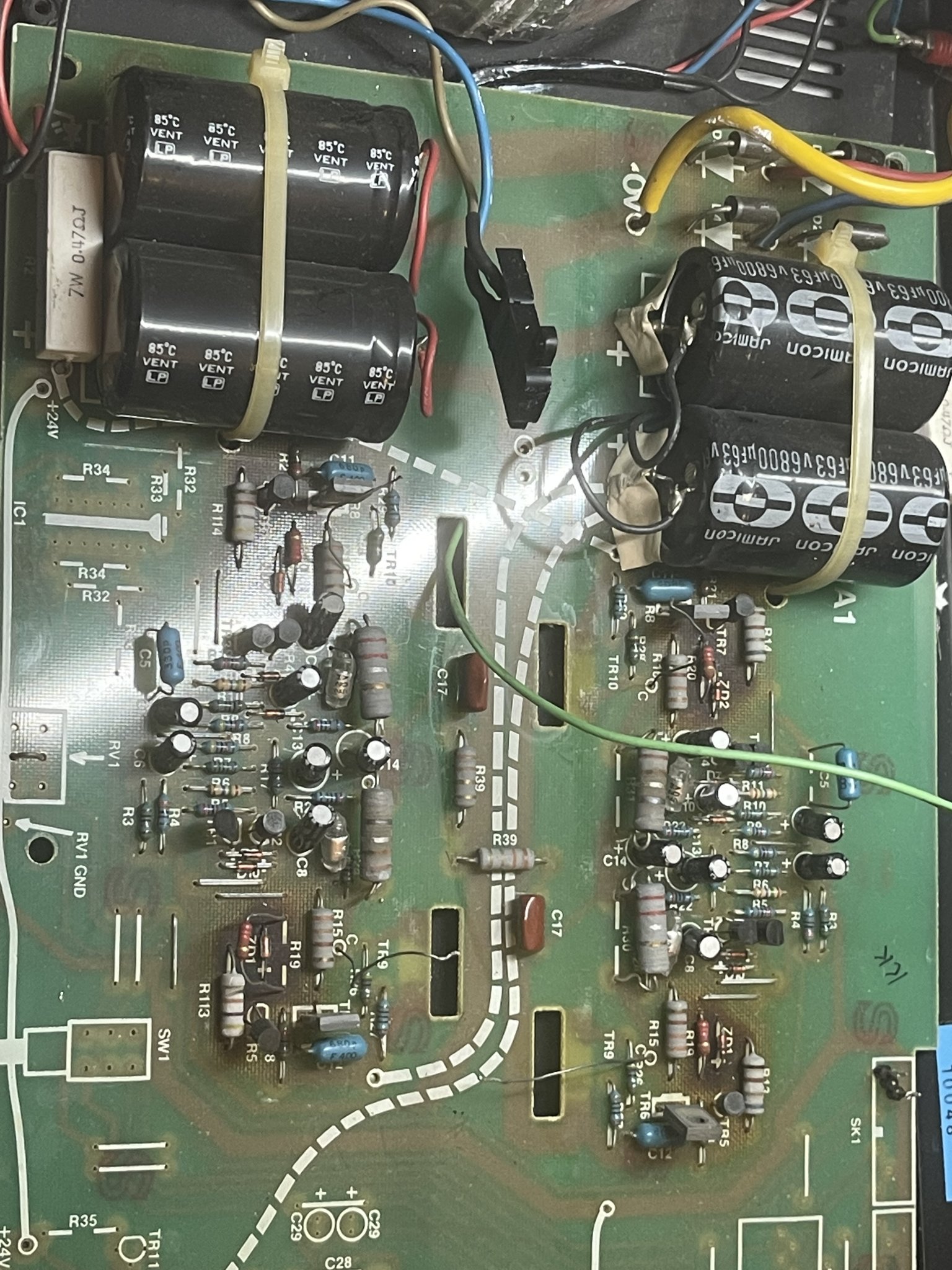
The MA50 is basically same circuit as A1.
It parallels the two channel of outputs together to make it mono.
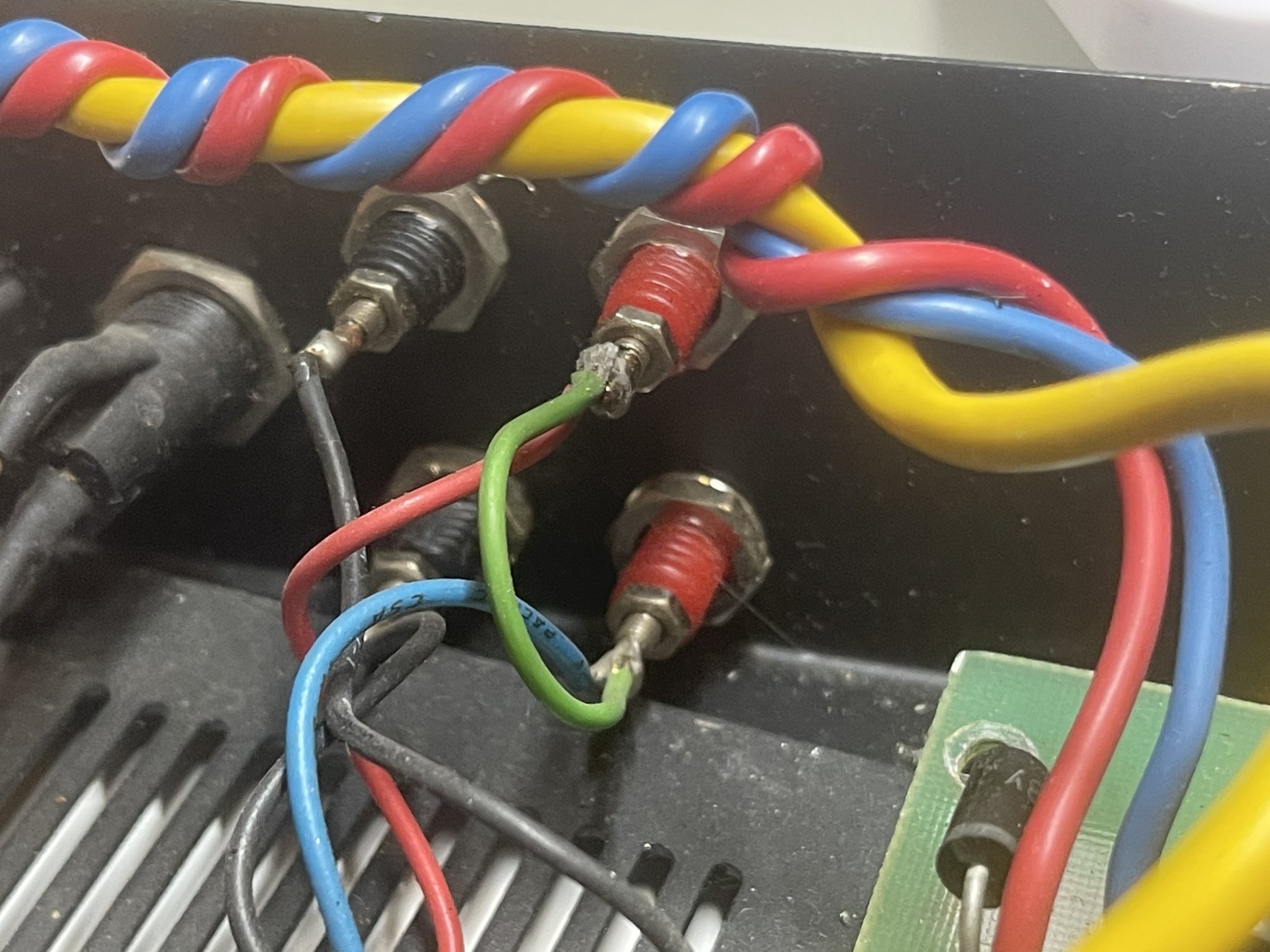
the way it parallels couldn’t be simpler, as you can see, it just uses a green wire to link two positive terminals together. Anyone can do the same to any stereo amp by just using a jump lead.
My question is wont the way they did to parallel cause a problem? If the two channels are imbalances in voltage, say due to ageing or something, wont it be causing current feeding from one channel to another?
Is any modifications possible to make it more reliable? Like using link in a diode in each of the channel output provides some protection?
That is a good and sure way to damage one or both amplifiers and cause phase shift distortion ans one amplifier fights against the other.
To place an amplifier in mono mode the correctway is to common the inputs, left and right. Both amplifiers will then see an identical signal and phase errors in the amplifiers will not be noticeable.
Whoever put that green wire on there needs to learn how to solder as well!
To place an amplifier in mono mode the correctway is to common the inputs, left and right. Both amplifiers will then see an identical signal and phase errors in the amplifiers will not be noticeable.
Whoever put that green wire on there needs to learn how to solder as well!
This is original soldering from the factoryThat is a good and sure way to damage one or both amplifiers and cause phase shift distortion ans one amplifier fights against the other.
To place an amplifier in mono mode the correctway is to common the inputs, left and right. Both amplifiers will then see an identical signal and phase errors in the amplifiers will not be noticeable.
Whoever put that green wire on there needs to learn how to solder as well!
OMG! More than one Mr Bodge has been at that one. I understand the need for brutally honest close-up pics but sometimes it reveals a bit too much and I get the sense from the scorch marks under the zeners and bits of old cap leads, that this amp has already suffered a long, hard life and tinkering. It would be a lot easier to start from scratch with your own clone build, done with a similar end result in mind to what you plan. Sure, it takes a long time to get up to speed on such a project but if all you're really after is bigger A1, running two in parallel doesn't do much for typical hi-fi speakers - it just allows more current to suit lower impedance speakers. If you have any that are say, 6R or lower, together they could then be useful .
May I suggest; either restore the A1 properly, fit a stereo pair of clone A1 kits inside or build them into a larger case for more power as I've done in the past. There are still some excellent sounding clones out there, based on much better audio power transistors and I thoroughly recommend them because there is also more useful power available, assuming your case can dissipate the extra heat as a mono amp or otherwise as a larger stereo one. It's also amazing how much cooler the amps run with proper deep finned heatsinks rather that just the top of a small, plain box.
Here is one inexpensive way to begin DIY, if assembly work isn't intimidating and you could use some soldering practice.
https://www.aliexpress.com/item/100...1;11.78;-1;-1@salePrice;AUD;search-mainSearchThis isn't the best board for a hot amp but its about cheap and having a wide choice of good power transistors in large packages for good heat dissipation.
Even if you're more into collecting and fixing things from the glory days of hifi, you'll still need lots of assembly practice to be good enough to pass on your work confidently and without fear of only gaining a lousy reputation.
Last edited:
Oops, thanks. I will re-solder it.I, for many years, ran an AR Cambridge Aurhorised Service Centre. I have worked on most models both in and out of warranty and can tell you, that is not original.
You need to remove it and wire the amplifier as I suggested before you get magic smoke!Oops, thanks. I will re-solder it.
MA50s are dual mono amplifiers, they come a pair, both wired like this. They have only one input each. I think they are designed like thisYou need to remove it and wire the amplifier as I suggested before you get magic smoke!
Yes they get burned. Its common problems with this ampAre my eyes deceiving me or are there several resistors that have gotten hot?
When a PCB is clearly charred, as in black and carbonised as the pics show, it's likely that the surrounding PCB tracks will now have whatever complex resistances the carbonised epoxy areas add between them. There will likely be too many complex resistance paths to track down and eliminate all effects and the only efficient way to deal with them is to replace the PCB with a good one - if actually available or economically reproducible.
All the same, I've seen a couple of A1s, other amps and a power supply that actually had been repaired by routing out the charred PCB sections with a Dremel or similar miniature drill/router tool, then patching with epoxy filler to restore a smooth, cleanable surface. It may seem a reasonable process but it's actually a lot of painstaking work. If restoration and resale is your game, this isn't the way to go but you don't have many options if there are significant current leakage paths that should not exist according to the circuit when you check the node voltages of a particular circuit section against a good, working channel or by running a SPICE simulation. "significant current" here, just means relative to any currents that should be flowing between circuit nodes, according to the schematic or sim.
All the same, I've seen a couple of A1s, other amps and a power supply that actually had been repaired by routing out the charred PCB sections with a Dremel or similar miniature drill/router tool, then patching with epoxy filler to restore a smooth, cleanable surface. It may seem a reasonable process but it's actually a lot of painstaking work. If restoration and resale is your game, this isn't the way to go but you don't have many options if there are significant current leakage paths that should not exist according to the circuit when you check the node voltages of a particular circuit section against a good, working channel or by running a SPICE simulation. "significant current" here, just means relative to any currents that should be flowing between circuit nodes, according to the schematic or sim.
- Home
- Amplifiers
- Solid State
- Musical Fidelity MA50 paralleled output question