Design of my 120 Watt amplifier
I thought it was time i made a amp myself, after more than 10 years repairing vintage audio amps.
This is the B revision. I did some measurements and listening test to the A revision and made some changes. When the PCB's come back i'll share some more pictures.
Also i'll share some snippets from the schematics and nifty things on the pcb.
Last edited:
Output stage is a CFP, with double power transistors. R27 and R34 are the stop resistors for the power transistors. R20 is the stop resistor for the driver transistor.
R29 and R38 are needed to balance the current between the 2 output transistors.
Q12 is the main component from the VI limiter. Maximum output current is dependent of the voltage across the power transistors. This ensures max use off the power transistors SOA. See the simulation for results.


R29 and R38 are needed to balance the current between the 2 output transistors.
Q12 is the main component from the VI limiter. Maximum output current is dependent of the voltage across the power transistors. This ensures max use off the power transistors SOA. See the simulation for results.
Because I have a CFP output stage the VBE multiplier needs to compensate the driver transistors only. Besides a lot of temperature simulations and real world measurements, I made a nifty PCB design.
Q11 is the VBE multiplier, the two TO220 transistors are the inputs of the CFP stages. When mounting they get folded on the "heatsink" integrated in the pcb. This ensures a very tight thermal coupling, and makes the quiescent current very stable.
The 2SA1837/2SC4793 are isolated, so no thermal pads are needed.
I have not examined your IV in detail.
But the 47k : 680r||1k seems to have set the Vbe of the protection very close to turning on the protection when no output current is passing.
The IV protection to be effective must allow all valid audio signals to pass to all valid audio loads.
I have a feeling that your protection transistor is by-passing a little bit of current that should be passing into the output transistor's base when a valid audio signal is passing.
If this base current is being bypassed that will cause significant distortion of the output signal.
Why does C6 not appear in the simulation?
Last edited:
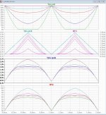
With 50V across the output transistor, current limiting starts at about 3A. This gives 150 Watts dissipation in the 2SC5200. That's just inside the SOA ")
For 2 output transistors value doubles, of course.
C6 was later added, after some simulating and real world testing. It makes the protection a bit smoother.
View attachment vi_limiter.asc
For 2 output transistors value doubles, of course.
C6 was later added, after some simulating and real world testing. It makes the protection a bit smoother.
View attachment vi_limiter.asc
Attachments

Last edited:
The 100ms one shot Tc=25°C SOA is ~4.3Apk @ 50VceWith 50V across the output transistor, current limiting starts at about 3A.
De-rate for elevated temperature and you may find that 3Apk is too high for a 1943.
Tc=65°C gives a derating factor of (150-65)/(150-25) = 0.68
Apply that to the ~4.3Apk from the cold SOA graph and you get ~2.92Apk for less than 100ms.
what current is passing the protection transistor when the output is 10mApk? 100mApk? 1Apk? and PSU is 52Vdc?
What if the prot transistor has warmed up during operation due to the internal Ta rising to 35°C. It's Vbe turn on voltage will be lower.
Last edited:
what current is passing the protection transistor when the output is 10mApk? 100mApk? 1Apk?
What if the prot transistor has warmed up during operation due to the internal Ta rising to 35°C. It's Vbe turn on voltage will be lower.
I think you are saying that the VI limiter adds up to distortion?
Actually, I did some simulations and it is adding distortion. For this board I found it acceptable, as distortions is very low. (120 W in 8 Ohm => 0.001988% @ 1kHz)
Somewhere in my head is this micro-controlled amp, that has adaptive bias, auto nulling servo and SOA protection that has no distortion.
Attachments

I am saying/defining a good IV as passing all valid audio signals to all valid audio loads.
If some base current is bypassed through the protection transistor, then you have changed the drive current. This bypassing action should not be allowed to happen when the signal is valid.
I think your Vbe when output current is very low is too close to (or even above) the minimum turn on voltage of the prot Q. i.e. the 680r is too high a value.
Looks a neat layout Johnny.
Is this a design you are going to share on the forum (circuit details/PCB layout etc), or is it one you hope to offer for sale ?
I have not decided yet. For sure I'll share the circuit details and the complete circuit diagram. And if the B revision is functional and to my satisfaction perhaps I will offer the remaining pcb's for a smal fee, to cover the cost of manufacturing.
Thanks.
The reason for asking was that once a venture looks like becoming commercial, then it would be placed in the Vendors section of the forum.
The same would also apply if circuit details weren't shared and so on.
Its nothing personal, we just have to treat (and be seen to treat) everybody the same over things like this.
@AndrewT: thanks for your input. A bit alarmed I decided to simulate the output stage with protection in a different way.
I noticed that the current thru the limiting transistor was to high, just as you said. The result was that the limiting was not "steep" enough.
I played with the resistor values, and did some calculations too
The result can be seen in the new simulation. The current through the limiting transistor is now 5 times lower.
With 8 ohm load, the current through the diode is 30nA top, so the signal passes unaltered.
With 4 ohm load the current is limited at about 9 amps. Voltage across the
power transistors is about 15V, giving 135 Watt total loss, or 67.5 Watt per transistor. No problem.
With 2 Ohm load the current is limited at about 7 Amps. Voltage across the transistors is about 39V giving 273 Watt total loss, or 136,5 Watt per transistor. Just within SOA.
With 0.01 ohm short circuit, current is limited at 5.4 Amps. Voltage across the transistors is about 53V giving 286 Watt total loss, or 143 Watt per transistor. Just within SOA.
View attachment vi_double_lim.asc
Attachments

Could you post the .asc?
I would like to see the effect of the capacitor.
My thoughts are:
Set the DC limiting condition to pass enough very low frequency current through a resistive dummy load that equals the load rating of the amplifier.
Then use the capacitor to delay the limiter for faster current peaks.
This allows the limiter pass to transient currents that exceed the DC ratings and make use of the enhanced SOA for short term loadings.
If the prot Q is thermally coupled to the output devices/heatsink, then you can make use of the changing Vbe due to temperature to change the limiting condition depending on the temperature of the surroundings. i.e. more current passes without limiting when Qprot temp is low and less current when high temp.
Last edited:
Could you post the .asc?
I already posted it, 2 posts ago
Interesting though about using the dynamic part of the SOA ..
edit: changed V2 in a pulse, and varied C1 a bit. When C1 is to small (< 1 nF) , the circuit oscillates. When C1 is to high (>100 nF) circuit is to slow, and peak current is to high.
Last edited:
I have found that for effective IV limiting that R7, 8 & 9 need to be much lower, by a factor of ~4.
I have not found a way to test the real amplifier to prove the IV limiter actually works as well as the simulation model predicts. Have you?
I have also not found a way to test the effectiveness of the capacitor delay.
I see the asc now, thanks. Downloaded.
I have not found a way to test the real amplifier to prove the IV limiter actually works as well as the simulation model predicts. Have you?
I have also not found a way to test the effectiveness of the capacitor delay.
I see the asc now, thanks. Downloaded.
Last edited:
There was some comment a few years ago on temperature compensation for the output device de-rating due to high temperatures.I already posted it, 2 posts ago
Interesting though about using the dynamic part of the SOA ..
edit: changed V2 in a pulse, and varied C1 a bit. When C1 is to small (< 1 nF) , the circuit oscillates. When C1 is to high (>100 nF) circuit is to slow, and peak current is to high.
Some said that varying the Qprot Vbe using thermal coupling would not be effective. I have not done any research on that since.
When the limiter is active in an operating amplifier, you will probably find it oscillates even without the added capacitor. Some Members confirmed when prodded into looking, that their protection did oscillate. They had not looked for it until I mentioned it.
There must be a loop in which we can add compensation to eliminate this oscillation. That may then make your finding stable as well.
100nF & 1k gives a 100us time constant.
I wonder if that gets the peak current close to that when using a 100us SOA value?
There must be a loop in which we can add compensation to eliminate this oscillation. That may then make your finding stable as well.
100nF & 1k gives a 100us time constant.
I wonder if that gets the peak current close to that when using a 100us SOA value?
Last edited:
- Status
- This old topic is closed. If you want to reopen this topic, contact a moderator using the "Report Post" button.
- Home
- Amplifiers
- Solid State
- Design of my 120 Watt amplfier