Hello,
This is just a brainchild amplifier I've been doing latelly.
Maybe it won't ever be real, but anyhow I've always liked to toy with Electronics...
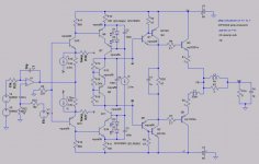
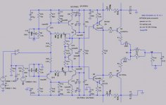
It's an OpAmp front end amp, using a super cascode and my pet triple output.
The compensation is not refined, it shows some peaks on heavy capacitive loads.
Notes:
There are 2 biasing diodes per base in the super cascode stage because I did not have a model for the green LED.
The BD139/140 pair was used just because I had the models (I know they will not stand the voltage).
The unusual 300nHy inductor in the output PNP emitter was the only way I've found to tame cross conduction. It may just be some limitation of the model.
Thanks for your comments,
This is just a brainchild amplifier I've been doing latelly.
Maybe it won't ever be real, but anyhow I've always liked to toy with Electronics...
It's an OpAmp front end amp, using a super cascode and my pet triple output.
The compensation is not refined, it shows some peaks on heavy capacitive loads.
Notes:
There are 2 biasing diodes per base in the super cascode stage because I did not have a model for the green LED.
The BD139/140 pair was used just because I had the models (I know they will not stand the voltage).
The unusual 300nHy inductor in the output PNP emitter was the only way I've found to tame cross conduction. It may just be some limitation of the model.
Thanks for your comments,
Attachments
Hi Jorge,
I think this needs a lot of work. The first stage of the discrete is not right! The 3K9 are way too high and should be more like 300R and that's a heavy load to drive from the chip. Also it's not good thermally as the biassing of this stage from CCS's tends to increase stage current at higher temperatures. Operating point stability is not good.
The cascode LED biassing and CFP drivers is as I used for the award winning Magnet amp (but with a comp diff FET cascode input stage).
Also the chip contributes only 20dB of gain at 20KHz where you need it most. Not the best compensation technique as it wastes GBW.
You asked.
Cheers,
Greg
Thanks, Greg
For your comments.
- I did not care for the opamp gain and loss in the CB stage very much because I already have about 40dB FB at 20K, crossing zero gain with 56 deg.
But from your words, it can be improved.
Can you elaborate on "the biassing of this stage from CCS's tends to increase stage current at higher temperatures"?
BTW, model CCIF IM (my favorite measurement) place all in band products at -100dB at 80V pp out..
A pity it's not real!
Regards,
Jorge
.
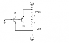
Hi Jorge,
I have attached a drawing for clarity. As temperature rises inside chassis the Vbe's drop and less current flows through the two R's. This current from the current sources is more and more deflected into the transistors Ic (to the next stage) as temp rises. Not really very good for overall thermal stability.
Cheers,
Greg
Attachments
Re: a lot of work
Dimitri
You're right about the 47 to 470 ohms change. Thanks for pointing it.
Re C7 - it helps (at least in simulation) to lower cross conduction of the outpt transistors (slow PNP).
LED for Zeners - not really necessary, the lower device of the cascode is happy with about 1V Vce, so an LED will do. I've used two reds because I don't have a model for a green one slightly more voltage).
dimitri said:R4=R5=470 not 47, otherwise IcQ1=IcQ4, why use Sziklai pair at all?
omit C7
xchange D1,D4 (D2,D3) on 4.7V Zeners
Dimitri
You're right about the 47 to 470 ohms change. Thanks for pointing it.
Re C7 - it helps (at least in simulation) to lower cross conduction of the outpt transistors (slow PNP).
LED for Zeners - not really necessary, the lower device of the cascode is happy with about 1V Vce, so an LED will do. I've used two reds because I don't have a model for a green one slightly more voltage).
Helo, Greg
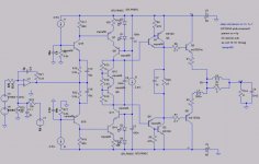
Here it is again.
- The common base stage now has a more standard biasing. The current sources are there just to easy PSRR measurements.
- I've kept the common base since even as it was OL gain is 90dB, so...
- I changed the super cascode to a plain cascode. For some reason LTSpice didn't like the PNP side of it...weird results.
- I've redone compensation as well as I could, but it wasn't possible to avoid some around the opamp. Maybe the BW of the bipolar stages (even oly the cascode) is too narrow?
- I've applied a fair ammount of phase lead using the CB emitters.
Here's the new diagram
Attachments
Re C7 - it helps (at least in simulation) to lower cross conduction of the outpt transistors (slow PNP).
Yes, you are right, but think about the path of discharge current and about correspondent voltage drop on the other side. Would you like to discharge quickly, add two more transistors.
LED for Zeners - not really necessary, the lower device of the cascode is happy with about 1V Vce, so an LED will do.
this is only simulation, in practice you need at least 3V across lower device, otherwise cascode distortion is much higher. Stick to soldering iron, not keyboard

Hi Jorge,
Yes that's a much more stable biassing for the common base stage - but look at the voltage loss in the stage. You indicated it wasn't of concern.
The following cascode stage - you can use a single LED for bias to the emitters of the CE part - this gives the lowest THD in my experience and as I used in the Magnet 300F.
Where's the global NFB?
Cheers,
Greg
Hello, Greg
Interesting - your single LED goes fully against Dimitri's pot above...
I've used a lot one LED to bias current sources.
The global FB is applied to V4 at the lower left of the circuit - label FB
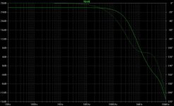
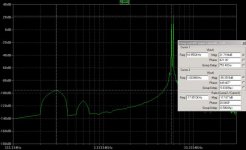
The gain graphic I've posted is just loop gain, not showing the 26dB of amp gain, so every value shall be increased by 26 dB for total gain.
At 100Hz there's about 160dB total and at 20k some 80dB total.
Feedback factor at 20k (shown in the graphic) is 54dB.
The Opamp has a gain of 80dB and a BW of 22MHz, so the bipolar stage adds another 80dB of the VAS stage.
That's why I don't care for the loss in the common base stage, I don't need gain - I need BW!
And a common base has a very wide BW.
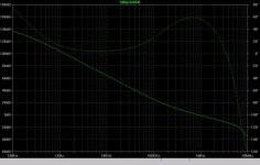
The PSRR was adjusted (using small inductors to avoid power loss) to some 100dB up to about 100kHz, when the output transistors capacitance starts to degade it.
Well, that's it.
The main advantage I see in using an Opamp as front end is that there's a hidden servo in the circuit.
Regards,
Jorge
Interesting - your single LED goes fully against Dimitri's pot above...
I've used a lot one LED to bias current sources.
The global FB is applied to V4 at the lower left of the circuit - label FB
The gain graphic I've posted is just loop gain, not showing the 26dB of amp gain, so every value shall be increased by 26 dB for total gain.
At 100Hz there's about 160dB total and at 20k some 80dB total.
Feedback factor at 20k (shown in the graphic) is 54dB.
The Opamp has a gain of 80dB and a BW of 22MHz, so the bipolar stage adds another 80dB of the VAS stage.
That's why I don't care for the loss in the common base stage, I don't need gain - I need BW!
And a common base has a very wide BW.
The PSRR was adjusted (using small inductors to avoid power loss) to some 100dB up to about 100kHz, when the output transistors capacitance starts to degade it.
Well, that's it.
The main advantage I see in using an Opamp as front end is that there's a hidden servo in the circuit.
Regards,
Jorge
Hi Jorge,
Hmm I see I'm at odds with dimitri. As I said "my experience" was that one LED returned to the emitter resistor was that lowest of the options I tried. I didn't try 2 LEDs for higher Vce as it would have directly compromised output and my THD was very low already. Maybe 'gilding the lily' .
Yes you're right about the 'free' servo! But it's thanks to the monolithic matched and temp tracking defined input stage - at lower cost and less hassle than doing it discrete, especially FET.
cheers,
Greg
Just a short comment/question...
I see alot of designers used a cap similar to your C6 but I can only imaging that it causes problems. In the very short term (a couple of cycles) it might help with cross conduction but when it does actually help it gets discharged quite fast. Then it takes time for it to recharge through the bias current. Whle this is recharging the output device bias is too low and crossover distortion can occur.
The way I test for this effect is to simulate a fairly long high frequency sine wave and look at the voltage across C6. If it drops over time thene will be a problem with bias after the hf burst stops. Your cap is fairly small so recharge might be fairly fast, but the effect is the same....
Doug Eleveld
Hello, Doug
You're right, I had forgotten this negative side effect of this cap...
I've simulated the circuit with and without the cap.
First I could only noticed an significant effect on clipping, the higher the frequency more significant it is. Bias will slide.
The sense of the slide (more or less bias) will depend on the real amp assimetry. It may be any way.
The larger the cap, the longer it takes to charge - and to discharge...
An iteresting test would be to connect an LP filter - say an 10K resistor and a 10u cap to an amp output and measure the output DC voltage with music. I'm betting the reading will change...
Now, the cap helps with transistor cross conduction, and makes bias slide more noticeable.
Hello Gorge,
I don’t understand why you changed the schematic around D1 – D4. In your first schematic I recognize the article of Malcolm Hawksford “Reduction of Transistor Slope Impedance Dependant Distortion in Large-Signal Amplifiers” in J. Audio Eng Soc., Vol. 36, No 4, 1988 April. You can find this article on the website of M. Hawksford:
http://www.essex.ac.uk/ese/research/audio_lab/malcolms_publications.html He proves why it is better to connect the diodes with the emitters and not with the supply voltages.
Why do you use an opamp for the input stage?
At the output you use a CFP combination as the driver and an EF configuration for the output transistor while the study and research of Douglas Self shows that a CFP configuration for the output transistor has the lowest distortion (but a little more vulnerable for oscillation especially with negative feedback). Why not an EF – CFP instead of a CFP – EF configuration?
Marc.
Hello, Mark
It started as a combination of Hawksford's super cascode as a VAS with an opamp input stage and the CFP/EF output (as per the first post of this thread, my pet output circuit).
I changed form super cascode to a classical cascode because the PNP side was giving LTSpice very hard time, completely weird results. No other reason.
I feel the real amp would benefit from the original topology.
Re the output stage, I have Self's book and find it interesting that although the CFP is the best, he doesn't uses it in the Blameless amp (but then he does in the Load Invariant).
Besides, I like output triples, so for me the combination of a CFP and an EF is the best possible triple (less Vbe drops to compensate termally/generate distortions).
The CFP was placed as a driver to help with the well known tendency of HF oscillations on CFP's by buffering it from the load.
Regards,
Jorge
- Status
- This old topic is closed. If you want to reopen this topic, contact a moderator using the "Report Post" button.
- Home
- Amplifiers
- Solid State
- Comments on Intelectual creation, pls