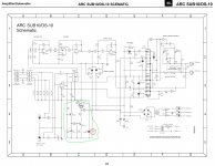
Hi, I bought a non-working class D, JBL ARC SUB10 to repair. After replacing some capacitors and a resistor it works now but I noticed another problem. Some glue from a hot glue gun that was covering a resistor had liquified from that resistor getting hot. Not hot enough to burn out the resistor, but enough to melt the glue around it. This happened before the capacitors burned out and when I power the amp it still heats up. It is the resistor R19 circled in red on the schematic. It is part of the circuit circled in green. At first I thought the green circuit was some sort of voltage regulator, but then I saw it was controlled by the audio signal which I thought was weird. Looking into it more I figured out the LED DRIVE was a 2 color LED that changed from red to green when I audio signal was fed through the amp and the circuit was some sort of auto 'power on' since there is no power switch.
This circuit confuses me. Could someone explain in simple terms how this circuit automatically turns the amp on and off?
And since this sub will be turned on and off by the power strip it will be plugged into, this circuit is not really necessary. Could I remove resistors R19, R20, and R21 and use it that way (always on unless unplugged)?
Thanks
Scott
Attachments
I don't see anything in that circuit section that does anything but drive the LED. Taking the resistors out would shut it down and take a funny load off the input buffer. You could rewire so you at least had a power indicator, but if there's signal level power control in the sub circuit, which is common, its not in the roped off section.
I am still kind of new at this so I didn't know if there was something I was missing when I was looking the circuit. The manual states that the LED colors were an indication of wether the amp was in standby mode or on. And that the amp switches from standby to on and back based on wether there is audio present.
Well I removed R19 and R20 but left R21 as your recommendation. Now the red LED lights when the amp is plugged in for a power indicator but the rest of the circuit is out.
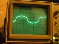
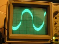
When I first got it working I could not check the sub at high volumes. At quiet levels it sounds great. Now I had a chance to test full volume. It sounded horrible. As soon as you turn the volume up and start to push the amp, it gets this weird honk to sound and you loose the deep bass. I know this sub can't sound this bad unless something is not right. So I hooked up a function generator and sent a 30Hz sine wave into it and checked with an oscilloscope. Everything looked good through the four sections of the LM324. Then on the input of the S53 Module the sine wave got very distorted. The output was really bad, not even a sine wave anymore. Totally compresses the signal. You can also see there is clipping going on at higher levels. When I turned the volume down (almost off) the waves got better which is what I observed listening at low volumes.
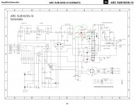
Now I've read about these modules having problems and dying, but they usually stop putting out sound. I took a voltage meter and checked around the module and found another problem. It is the +6V Supply. I circled it on the schematic and I listed some of the voltages readings I took.
You can see by the readings that there does not seem to be a +6V supply. It seems the +6V would come from the positive rail through R9 and then D6 (which is a 6.2V zener diode) would set the voltage at +6.2V. This would work nicely if the other end of diode was connected to ground. But it is connected to the negative rail instead which caused the cathode side of the zener to be 6.2V up from -44.5V. That matches my readings of -38V. I also measured around the zener and got a 6.2V difference so D6 is working properly.
It looks like if D6 was connected to ground I would see +6V there. Is there something I am missing here?
Scott
Well I removed R19 and R20 but left R21 as your recommendation. Now the red LED lights when the amp is plugged in for a power indicator but the rest of the circuit is out.
When I first got it working I could not check the sub at high volumes. At quiet levels it sounds great. Now I had a chance to test full volume. It sounded horrible. As soon as you turn the volume up and start to push the amp, it gets this weird honk to sound and you loose the deep bass. I know this sub can't sound this bad unless something is not right. So I hooked up a function generator and sent a 30Hz sine wave into it and checked with an oscilloscope. Everything looked good through the four sections of the LM324. Then on the input of the S53 Module the sine wave got very distorted. The output was really bad, not even a sine wave anymore. Totally compresses the signal. You can also see there is clipping going on at higher levels. When I turned the volume down (almost off) the waves got better which is what I observed listening at low volumes.
Now I've read about these modules having problems and dying, but they usually stop putting out sound. I took a voltage meter and checked around the module and found another problem. It is the +6V Supply. I circled it on the schematic and I listed some of the voltages readings I took.
You can see by the readings that there does not seem to be a +6V supply. It seems the +6V would come from the positive rail through R9 and then D6 (which is a 6.2V zener diode) would set the voltage at +6.2V. This would work nicely if the other end of diode was connected to ground. But it is connected to the negative rail instead which caused the cathode side of the zener to be 6.2V up from -44.5V. That matches my readings of -38V. I also measured around the zener and got a 6.2V difference so D6 is working properly.
It looks like if D6 was connected to ground I would see +6V there. Is there something I am missing here?
Scott
Attachments
For some reason it seems the amp module needs a 6 volt reference off the - supply. I don't know what it's doing with it but from your measurements it doesn't look broken.
What a circuit. With a 2.2M resistor on that 30V zener, D1, seeing exactly what's going on at the shutdown pin could be hard with just a DVM. (scratch that, I forgot reading you have a scope. What's it look like on the scope [you'll definitely need a x10 probe and it will still drag the voltage there a bit]). The impedance at the collector of Q3 should likely stay very high in normal operation. You should likely never see the minus supply from the shutdown pin. Do you get any voltage movement on the shutdown pin under drive? What is that voltage? Are those .1 ohm resistors healthy? How about solder connections there? Can you get any data on the module?
If you wind up proving the current limit/ shutdown circuit is healthy, the module is probably baked.
That shutdown circuit probably gets a lot more active with lower currents on the sense resistors if temperture rises very much, not that this is an issue here.
Last edited:
I could be wrong. The fact that they chose a high speed switch for Q3 could mean they intend for it to swing to the minus supply. It could definitely do that very quickly by discharging C3 if Q3 got more than .6 volts across the base. And it would recharge comparatively slowly when the current dropped below the switch threshold. The shutdown speed is probably the biggest reason they chose such a high impedance at the S/D pin, so they could set up the time constant they wanted on the UVLO and protection recovery, and shutdown speed, and not need a very high current protection switch transistor/circuit.
Last edited:
The potted power module used in this subwoofer and shown in the schematic (or a very similar one) has been already reverse engineered and repaired by a few people. Search for threads about JBL PB12 in the class D section.
Edit: Found the thread --> http://www.diyaudio.com/forums/class-d/48627-jbl-pb12-subwoofer-class-d-amp-dead.html#post542253
Edit: Found the thread --> http://www.diyaudio.com/forums/class-d/48627-jbl-pb12-subwoofer-class-d-amp-dead.html#post542253
Last edited:
Ok so their +6V is referenced from the V-. I am just used to something labeled +6V would actually be +6V, not -39V.
Thanks Eva for the link. The BP12 is very similar to the SUB10. They use the same type of module only with different V+ and V-. I was looking at the PB12 service manual and it has some test point voltage readings around the module that the SUB10 service manual did not. The S/D pin was -39.3V and that is +5.2V from V-. The test point reading for that is +5.1V from V- so that checks ok.
When I turn the gain from minimum to full on, the -39V on S/D drops to -38.6V.
Checking the S/D with the oscilloscope showed a 30Hz distorted triangle wave at full gain and with the gain turned down there are small triangles/ramps at around 150Hz.
When I removed R19 and R20 I just checked around afterwards with a voltage meter. Everything looked the same so I didn't check with the scope. Now I looked at the scope and the input to the S53AMI module the sine wave looked the same and was still distorted. But the output now looks much better. It looks like the input only more gain and less focused.
I put the amp back in the sub and tested how it sounds. The weird honk is still there but the volume is louder now. Rattles some stuff on the walls. It still seems like it should be louder for 100 watts.
I don't know if the changes are really from removing the resistors or from something like intermittent connection/solder joint. The first post in that link talks about factory rework. This board also has this. You can see where they resoldered a bunch of solder points. This make me think they were having a problem with cold solder joints. Then the SUB10 manual said I should resolder all the connections to the S53 module when I first replaced the bad capacitors.
The .1ohm resistors check ok. I resoldered all the joints in the short circuit protection circuit. Tested after showed no change.
The SUB10's module S53AMI is the less power version of the PB12's S64AMI module.
Scott
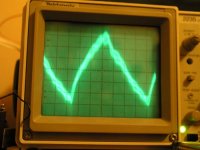
Here are some pictures of the oscilloscope.
1.Sine wave at amp input.
2.Sine wave at module input.
3.Sine wave at module output.
4.S/D pin with gain turned down.
5.S/D pin with gain turned up full.
1.Sine wave at amp input.
2.Sine wave at module input.
3.Sine wave at module output.
4.S/D pin with gain turned down.
5.S/D pin with gain turned up full.
Attachments

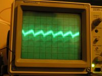
Ok what I thought was a trace to the modules input was actually from the last stage of the LM324 chip. I am still kind of new at this.
The attached picture is what I get on the scope at the modules input. It's double straight lines. This confuses me.
I am going to look into the last stage of the LM324 and the distortion.
Scott
The attached picture is what I get on the scope at the modules input. It's double straight lines. This confuses me.
I am going to look into the last stage of the LM324 and the distortion.
Scott
Attachments
Seeing that the last stage of the LM324 had distorted output, I checked around internet and found out that this is a very low quality op amp. Thinking that this distortion was the crossover distortion that this chip is famous for, I ordered a TL074. After installing the chip and testing I saw the same distortion.
Poking around some more I found inside 'Diode Clipper' circuit that resistor R13 was physically loose. Still soldered to the pads but the pads were not longer attached to the tracks. And the other side of the Diode clipper was not functioning properly ether. So this circuit was clipping the signal like a guitar distortion pedal!
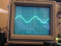
I installed new resistors and a few jumpers to get everything connected again. I hooked up the scope and the distortion was gone. The output look good so I put the amp back into the sub and tried it out. It sounds much better. Able to rattle the walls nicely.
I'm not completely happy withe the sound of the low pass filters. I would like it to roll off sharper. I am going to adjust the '700Hz Lo-Pass' filter down to around 50Hz. The other thing I am going to try is a notch filter to cut around 45Hz to level the resonance around there.
The more I look into this amp, the more I realize it is a piece of crap. Very low quality all around. Even something major like the labeling of the + and - for the speaker wires printed wrong on the PCB was not caught. And the PCB is so delicate that if you look at it wrong the pads will come right off.
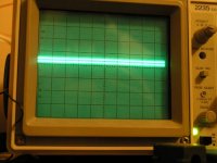
One last thing. Attached are a couple of pictures of the output of the TL072 and output of the S53 module. Since this amp is so cheap, I figure this is unique to this amp. But does anyone have any idea why the output trace from the S53 would be thicker then the output of the TL074 trace? Could it be low quality output inductors?
Thanks
Scott
Poking around some more I found inside 'Diode Clipper' circuit that resistor R13 was physically loose. Still soldered to the pads but the pads were not longer attached to the tracks. And the other side of the Diode clipper was not functioning properly ether. So this circuit was clipping the signal like a guitar distortion pedal!
I installed new resistors and a few jumpers to get everything connected again. I hooked up the scope and the distortion was gone. The output look good so I put the amp back into the sub and tried it out. It sounds much better. Able to rattle the walls nicely.
I'm not completely happy withe the sound of the low pass filters. I would like it to roll off sharper. I am going to adjust the '700Hz Lo-Pass' filter down to around 50Hz. The other thing I am going to try is a notch filter to cut around 45Hz to level the resonance around there.
The more I look into this amp, the more I realize it is a piece of crap. Very low quality all around. Even something major like the labeling of the + and - for the speaker wires printed wrong on the PCB was not caught. And the PCB is so delicate that if you look at it wrong the pads will come right off.
One last thing. Attached are a couple of pictures of the output of the TL072 and output of the S53 module. Since this amp is so cheap, I figure this is unique to this amp. But does anyone have any idea why the output trace from the S53 would be thicker then the output of the TL074 trace? Could it be low quality output inductors?
Thanks
Scott
Attachments

- Status
- This old topic is closed. If you want to reopen this topic, contact a moderator using the "Report Post" button.
- Home
- Amplifiers
- Class D
- Circuit questions