I am incredibly proud to announce I have made an amplifier with a schematics I have dreamt for a long while. I have only done very preliminary tests which are excellent. I have not yet written up the document, but, I am impatient to provide this information.
At present, the document contains the schematics only and will be updated, hopefully, soon.
Here is the link : Amplifier - Google Drive
Please, note : there are a lot of N. E. ( Not Equipped ) components. The reason to be on the schematics will be explained.
At present, the document contains the schematics only and will be updated, hopefully, soon.
Here is the link : Amplifier - Google Drive
Please, note : there are a lot of N. E. ( Not Equipped ) components. The reason to be on the schematics will be explained.
Steven, I assume you have picked transistors that are available in a metal case because you like the appearance but these are RF transistors and you could pick more appropriate ones for audio that are less likely to wind up with unwanted behaviour. BD139/140 would probably do nicely.
'Nice effort with drawing package though.
'Nice effort with drawing package though.
Steve are you aware that your output stage has no bias and thus will show appreciable cross-over distortion?
In fact, with the 100mA current capability of the opamp you probably don't need the output stage at all, depending on the load you want to drive. What is this amplifier meant for?
Also, the input impedance of 620 ohms is very low and will load down heavily on your source, not a Good Thing!
Jan
In fact, with the 100mA current capability of the opamp you probably don't need the output stage at all, depending on the load you want to drive. What is this amplifier meant for?
Also, the input impedance of 620 ohms is very low and will load down heavily on your source, not a Good Thing!
Jan
Last edited:
Interesting circuit. Inspired me to take a look at the datasheets.
The output of the LM7171 is very resonant into a capacitive load of the order of 100pF, possibly becoming unstable in the 50MHz region. I'd worry about that myself. A ferrite bead probably needs to be deployed to isolate the opamp's output from any capacitive load.
That opamp looks like its designed to drive 50 ohm stripline, not audio output devices!
I note its high current voltage swing is rather limited at +/-10V or so.
Alas the noise performance of the LM7171 at audio frequencies is poor. Being an RF device the 1/f knee is way up at 10kHz, so that voltage noise at 20Hz is about 60nV/sqrt(Hz), which could be popcorn or flicker noise or a combination of both. Popcorn noise would be bad!
With 9V rms (about the maximum usable at +/-15V supplies, you need to handle 1.1A or more to drive an 8 ohm load - those transistors can't take that. But then the output swing limits of the opamp mean 7Vrms is actually the practical max output, even so the transistor current handling is going to limit the performance.
I note the extremely low current gain of the output devices at high current, and therefore the large variation of gain with current through the cycle, basically a non-linearity.
The class BC output stage will of course have crossover, and even with a high speed feedback path to sort that out, its a glaring issue.
[ I say BC because the transistors will not be conducting for the full half-cycle duration ]
The CMRR of the LM7171 is fairly low at 70dB or 75dB worst case, but that might only be at RF frequencies. I note the distortion graphs seem to be OK at audio frequencies. The very low open-loop gain is notable as that will limit the ability to reduce the cross-over distortion, especially at low signal levels.
Unlike many amps this design is likely to hold its properties upto the MHz region due to the frequency response of the parts. The very large input capacitor would help prevent spurious HF junk getting into it, but it still seems extreme and the very low input impedance is unusual for audio.
Steven, I assume you have picked transistors that are available in a metal case because you like the appearance but these are RF transistors and you could pick more appropriate ones for audio that are less likely to wind up with unwanted behaviour. BD139/140 would probably do nicely.
'Nice effort with drawing package though.
The main reasons to pick these transistors are
* Their low parasitic capacitance values and, therefore, a fast jump switch from - 0.7V to 0.7V, i. e., their speed.
* Power of 1W to 1.5W, 1.2W OK.
* Possible to use a standard heat sink.
The disadvantage of these transistors is :
* High Ucesat.
* Max Icerms and Iberms of 0.4A. Not so bad.
* Very low B of 5 at high currents.
These transistors are, therefore, only for lower power, yet, higher than the amplifier.
The newly published document addresses these issues : Amplifier – Google Drive
Steve are you aware that your output stage has no bias and thus will show appreciable cross-over distortion? <snip>
The output current has been addressed in the previous reply.
The most important feature of the amplifier is to provide a general feedback which increases the speed of the jump and increases linearity.
620Ohm is one of the standards for audio, although very old. However, a preamplifier is supposed to be able to handle such an impedance. The best is to include the preamplifier in the same circuit. I have decided to have them separate in this stage. Own design preamplifier is to be used.
Headphone outputs can drive 32Ohm loads, sure they can do 620Ohm.
The low input resistor Ri is for :
* Comparable offset voltage to the one introduced by the feedback.
* To allow preamplifiers with DC filter capacitors which will not be charged by the bias current.
Obviously, the input resistor can be easily changed to the standard 10K and another 10K resistor can be added in series to the positive input for protection. This introduces offset which is OK for low gains and output DC filter capacitors which have been removed in the new version.
The whole idea of the output stage is not to be biased. The crossover distortion is not present with output capacitor from emitters to ground as well as with high quality power supply capacitors. This is addressed in the new document : Amplifier – Google Drive
Interesting circuit. Inspired me to take a look at the datasheets. <snip>
LM7171 is excellent with capacitive loads and does not show any instability even at a gain of 2. Looks like there may be switching noise in the audio range, through, which has been dealt with with an extremely low ESR capacitors from emitters to ground. This is discussed in the new document.
LM7171 is perfect for audio with very low noise. Of course, there are other amplifiers with even lower noise. Some of them may have a good slew rate too. TI has an amplifier with a guaranteed minimum slew rate of 50V/us. There are other too. The problem with LM7171 is the huge dependence of the slew rate on the size of the input signal. Thus, the input signal best come from a preamplifier with extremely low output impedance. At low input signals, the slew rate may be 700V/us. There are many other amplifiers with this slew rate, even fully differential ones.
Some test have been done with OPA134 and have been OK.
High frequency transistors have low parasitic capacitance and will not load the amplifier in normal work, only during part of the jump, even this is not strong because of the analogue nature of the jump. This is addressed in the new document. High frequency transistors can be used as capacitive buffers in Darlingtons with high power, high capacitive power transistors. This is also addressed in the new document.
The limitation of the input voltage is 10V pin to pin, but, with + - 15V power supply, the input voltage must be <= 7V anyway, and this is from the positive input to ground. Same voltage would be applied to the negative pin by the feedback. Even when out of regulation, the feedback would provide 15V * R1 / R2 to the negative pin, which is supposed to be OK for low gains.
Protection can be made but has not been used and the amplifiers are OK.
Another disadvantage of LM7171 is the reduction of the output voltage with the output current. Thus, high B transistors should be used for high power. There are Toshiba transistors with something like 100 or 200 B at 3.3A.
The input current noise at 10Hz is 10pA/SQRT(Hz). The input voltage noise at 10Hz is 100nV/SQRT(Hz). The input voltage noise is higher than the desired 1 to 15nV/SQRT(Hz), but, the amplifier is supposed to be used for low gain of 2 to 10, possibly 2 to 5. For all other parameters, I am prepared to sacrifice the input voltage noise at these low gains which is not audible.
The maximum voltage swing and, thus, the maximum power with the new transistors have been addressed in the new document. Again, Toshiba power transistors have extremely high B at high currents and can be used or Darlingtons can be used too. This has been addressed in the new document.
Crossover is not supposed to be present with the output capacitor from emitters to ground as well as with high quality audio power supply capacitors. This is the same for all amplifiers. This one introduces digital switching noise, of course, which can be dealt with in a standard way.
The CMRR, PSRR and the open loop gain of LM7171 are OK. There are amplifiers with higher values, but, this on is OK too. The power supply must have large audio capacitors. Switching power supplies are also possible, they must also have large audio capacitors. I have used linear power supplies and batteries only. I do have a switching power supply which I may use with external capacitors.
The input capacitor has been removed. Hopefully, the preamplifier would have good filters. Again, the preamplifier must be incorporated in the design. For this design, I am interested in the amplifier part. I use self made preamplifiers as well as the headphone output of a Sony radio.
The biggest problem has been the switching noise, the others are OK and not audible. The switching noise has been eliminated as per the document.
The amplifier has not been tested at extremely high power. No high power power supply except eight 10A/h 3.7V batteries. No possibility to output high power. High power 4Ohm resistors can be used for tests. Not real tests though and no oscilloscope, no any other instruments. Cannot crank up the volume in the present environment.
Again, all addressed concerns are OK except the switching noise which has been high but eliminated.
The new document is at : Amplifier – Google Drive
There have been many versions and changes since I started this topic. Here is the document : Amplifier – Google Drive
What about "not to be biased" ===> "almost not biased" ?The whole idea of the output stage is not to be biased.
With the addition of two (or maybe three?) shottky diodes and two resistors, would an "almost not biased" version provide additional benefits in terms of lower switching distortion?
As instead of switching 1,4V .... reducing this switching range to a "lesser value" of switching volts?
A smaller "switching delta". Smaller hysteresis.
{{ this is not a fleshed out schematic detail - just the "general idea" }}
... if, for example, you find a low forward voltage diode, Schottky type, such as with a forward voltage of 0,45V, then two of such total 0,9V, hence potentially decreasing the switching / hysteresis region from 1,4V down to 0,5V.
Each output transistor would be slightly pre-biased, with 0,45V, which is basically insufficient to turn it on, except for maybe a trickle (non-critical) standing current, and I am guessing that it would be of a value in the miliamps range.
Further, I would consider co-locating the Schottky diodes on the output transistors themselves, so as to achieve good thermal tracking. If using a TO-247 / TO3P / TO-264 enclosure type device, this would be easy - simply bolt the Schottky diode down directly to the top side of the transistor enclosure, with some thermal grease coupling them.
Not sure how to ensure good thermal tracking with the currently used transistors though. Adjacent on same heat-sink, would be the next best guess.
Attachments
I'd be interested to see a graph of distortion against output level for 1kHz and 20kHz. When the output level is small the very low transconductance of the OS may lead to a big jump in distortion - the open loop gain must vary significantly with drive level in such a design.
[BTW the lack of need for biasing or temperature compensation is great - but can you really get away with that lack of bias?? Have you considered adding a capacitor from opamp output direct to the main output to reduce the switching transient slew rate? This might allow the feedback loop more control during this transition - however this has to be balanced against the heavy drive the LM7171 has to provide (it sees the 8 ohm load at higher frequencies).]
[BTW the lack of need for biasing or temperature compensation is great - but can you really get away with that lack of bias?? Have you considered adding a capacitor from opamp output direct to the main output to reduce the switching transient slew rate? This might allow the feedback loop more control during this transition - however this has to be balanced against the heavy drive the LM7171 has to provide (it sees the 8 ohm load at higher frequencies).]
Last edited:
What about "not to be biased" ===> "almost not biased" ? <snip>
Another variation of this schematics is a common emitter transistor and diodes. This is a standard approach in OA design.
The idea to add some bias, but, not full as with Schottky diodes is OK as far as power consumption is concerned. However, the introduction of resistors is something I would like to avoid as well as the parasitic capacitances of the diodes which can be low with low power Schottky diodes, but, then, the resistors must be high.
Also, this will only half the jump which is will not save very much even with Darlingtons.
... if, for example, you find a low forward voltage diode, Schottky type, such as with a forward voltage of 0,45V, then two of such total 0,9V, hence potentially decreasing the switching / hysteresis region from 1,4V down to 0,5V. <snip>
The document discusses the non linearity in space ( amplitude ) and time ( half period ). The greater the frequency, the higher the nonlinearity. However, when the jump is completed for t ( the goal is 250ns ), the relative error to the amplitude is :
( Asin(wt) / A ) * 100 %
This can be calculated for any frequency. The document shows a calculation for 20kHz. The nonlinearity error is 5% for 1% of the half period ( 25us ).
This is only in case the jump completes for 250ns.
As the document says, I do not have any equipment to measure this.
In regards to a possibility to increase Ceb with a capacitor from bases to emitters, I have tried this, but, I do not want to slow the charge of Ceb, on the contrary, I want to speed this up and prefer to use an output capacitor Co instead.
Yes, capacitor Ceb and Reb do slow the transistor. Reb limits the range and can be used with Darlingtons. Ceb does not help with the noise unless the value is huge ( 10uF as far as I remember ) and seems to introduce even more noise. I used the Ceb of the transistors with resistors from 10 Ohms to 1K and OPA134. 1K worked extremely well resulting at perfect sound. Of course, again, the voltage over the 1K resistor lowers the range.
Also, I have tried to avoid any resistors and capacitors. I would not put Co in case possible. I have not tried the new configuration without Co, but, with the old configuration ( 1% resistors and a resistor from the amplifier's output to ground ) was incredibly noisy. This is why a VERY LOW ESR Co was needed. 1uF did the jobe with the old schematics and I decided to use this on the new ( lower noise ) schematics just to be more sure. Did not do more experiments.
Co is 1uF, 100V, X7R. 100V X7R has lower ESR and ESL than 50V X7R or so I have seen.
Yes, this is the switching noise described in the document. Seems to be OK with Co and Csi.Doesn't a complementary-transes-pp-design just make noise;-?!
I cannot measure the sound in any other way, except by ear. As the document says, sounds perfectly. I heard sounds on songs which I never heard before, although I listened to these songs for decades.
OK, ... so strike the resistors.Another variation of this schematics is a common emitter transistor and diodes. This is a standard approach in OA design. <snip>
How about a floating current source, from a totally separate set of transformer windings, that provide a constant and steady current across those two or four under-bias diodes of mine? And since separate and floating, such current from current source could be actually set per preference, as to what the circuit would work best with.
...
Yeah, I know, slight overkill, a separate floating circuit and all, but maybe the distortion specs could be improved significantly? Would it be possible to simulate this scenario and see if it gives a chance for value added?
Again : I am happy with Co and Csi also because, for the new schematics, a lower value may be possible to be used. Also, I can add external capacitors, as I have, in a separate module.
Also, I have tried to make the direct schematics work : amplifier and two buffer, common collector transistors only. No common emitter transistor with a resistors, no diodes with resistors. This has been explained in other threads I have opened.
The only thing I had to use is Co which may or may not be necessary. Co, also, may or may not be necessary with other parts, mainly, transistors.
The jump creates an error of nonlinearity, or, distortion. The faster the jump the lower the error.
The document discusses the non linearity in space ( amplitude ) and time ( half period ). The greater the frequency, the higher the nonlinearity. However, when the jump is completed for t ( the goal is 250ns ), the relative error to the amplitude is :
( Asin(wt) / A ) * 100 %
This can be calculated for any frequency. The document shows a calculation for 20kHz. The nonlinearity error is 5% for 1% of the half period ( 25us ).
This is only in case the jump completes for 250ns.
As the document says, I do not have any equipment to measure this.
In regards to a possibility to increase Ceb with a capacitor from bases to emitters, I have tried this, but, I do not want to slow the charge of Ceb, on the contrary, I want to speed this up and prefer to use an output capacitor Co instead.
Yes, capacitor Ceb and Reb do slow the transistor. Reb limits the range and can be used with Darlingtons. Ceb does not help with the noise unless the value is huge ( 10uF as far as I remember ) and seems to introduce even more noise. I used the Ceb of the transistors with resistors from 10 Ohms to 1K and OPA134. 1K worked extremely well resulting at perfect sound. Of course, again, the voltage over the 1K resistor lowers the range.
Also, I have tried to avoid any resistors and capacitors. I would not put Co in case possible. I have not tried the new configuration without Co, but, with the old configuration ( 1% resistors and a resistor from the amplifier's output to ground ) was incredibly noisy. This is why a VERY LOW ESR Co was needed. 1uF did the job with the old schematics and I decided to use this on the new ( lower noise ) schematics just to be more sure. Did not do more experiments.
Co is 1uF, 100V, X7R. 100V X7R has lower ESR and ESL than 50V X7R or so I have seen.
Also, forgot to mention again : as mentioned in the document, another difference between this circuit and a standard amplifier is Co introduces a frequency dependent resistance ( impedance ) of 1 / jwCo which is 8 Ohms at 20kHz and 5.33 Ohms at 30kHz. With RL = 4 Ohms, the amplifier will see not 4 Ohms but 4 || 8 = 2.67 Ohms at 20kHz and 4 || 5.33 = 2.28 Ohms at 30kHz. The amplifier must be able to handle these resistances. The amplitude of these frequencies is normally very low with audio signals.
Of course, the introduction of a frequency dependent resistance introduces problems with linearity, which, hopefully, are negligible.
Otherwise, yes, there are very many possibilities as discussed in other thread I have posted. Also, I have mentioned the standard approach : amplifier, common emitter transistor with only Rc, two Schottky diodes ( can be omitted ), transistors.
There are many variations of this standard solution. There have been many updates to the document since last posted. Here is the document again :Amplifier – Google Drive
The transistors will allow for a larger current flow when the output transistors are fully or close to fully open. During the jump, they are not so important as not so much current is needed.
Again, I have not checked the schematics, hopefully, I have not made a logical mistake.
EDIT: Collector resistors of T11 and T21 OK, but, not needed.
Also, I have tried to make the direct schematics work : amplifier and two buffer, common collector transistors only. No common emitter transistor with a resistors, no diodes with resistors. This has been explained in other threads I have opened.
The only thing I had to use is Co which may or may not be necessary. Co, also, may or may not be necessary with other parts, mainly, transistors.
The only problems this circuit has is the jump. The rest is the same as with every other amplifier.I'd be interested to see a graph of distortion against output level for 1kHz and 20kHz. <snip>
The jump creates an error of nonlinearity, or, distortion. The faster the jump the lower the error.
The document discusses the non linearity in space ( amplitude ) and time ( half period ). The greater the frequency, the higher the nonlinearity. However, when the jump is completed for t ( the goal is 250ns ), the relative error to the amplitude is :
( Asin(wt) / A ) * 100 %
This can be calculated for any frequency. The document shows a calculation for 20kHz. The nonlinearity error is 5% for 1% of the half period ( 25us ).
This is only in case the jump completes for 250ns.
As the document says, I do not have any equipment to measure this.
In regards to a possibility to increase Ceb with a capacitor from bases to emitters, I have tried this, but, I do not want to slow the charge of Ceb, on the contrary, I want to speed this up and prefer to use an output capacitor Co instead.
Yes, capacitor Ceb and Reb do slow the transistor. Reb limits the range and can be used with Darlingtons. Ceb does not help with the noise unless the value is huge ( 10uF as far as I remember ) and seems to introduce even more noise. I used the Ceb of the transistors with resistors from 10 Ohms to 1K and OPA134. 1K worked extremely well resulting at perfect sound. Of course, again, the voltage over the 1K resistor lowers the range.
Also, I have tried to avoid any resistors and capacitors. I would not put Co in case possible. I have not tried the new configuration without Co, but, with the old configuration ( 1% resistors and a resistor from the amplifier's output to ground ) was incredibly noisy. This is why a VERY LOW ESR Co was needed. 1uF did the job with the old schematics and I decided to use this on the new ( lower noise ) schematics just to be more sure. Did not do more experiments.
Co is 1uF, 100V, X7R. 100V X7R has lower ESR and ESL than 50V X7R or so I have seen.
Also, forgot to mention again : as mentioned in the document, another difference between this circuit and a standard amplifier is Co introduces a frequency dependent resistance ( impedance ) of 1 / jwCo which is 8 Ohms at 20kHz and 5.33 Ohms at 30kHz. With RL = 4 Ohms, the amplifier will see not 4 Ohms but 4 || 8 = 2.67 Ohms at 20kHz and 4 || 5.33 = 2.28 Ohms at 30kHz. The amplifier must be able to handle these resistances. The amplitude of these frequencies is normally very low with audio signals.
Of course, the introduction of a frequency dependent resistance introduces problems with linearity, which, hopefully, are negligible.
As mentioned, I am only interested in the direct circuit : amplifier and two common collector buffer transistors. Nothing else.OK, ... so strike the resistors. <snip>
Otherwise, yes, there are very many possibilities as discussed in other thread I have posted. Also, I have mentioned the standard approach : amplifier, common emitter transistor with only Rc, two Schottky diodes ( can be omitted ), transistors.
There are many variations of this standard solution. There have been many updates to the document since last posted. Here is the document again :Amplifier – Google Drive
Although I am only interested in the direct circuit and not in any other, as mentioned in the previous reply, I decided to try to make your idea not so much resistors dependent, because, your idea is brilliant and is not so standard. I used a standard approach of replacing resistors with transistors and, although I have not had the possibility to check the circuit logic, I have decided to post, because your idea is brilliant. I also do not remember to have discussed your idea in previous posts.What about "not to be biased" ===> "almost not biased" ? <snip>
The transistors will allow for a larger current flow when the output transistors are fully or close to fully open. During the jump, they are not so important as not so much current is needed.
Again, I have not checked the schematics, hopefully, I have not made a logical mistake.
EDIT: Collector resistors of T11 and T21 OK, but, not needed.
Attachments
Interesting development. I think that I "feel" where this concept is intended to be going, but I am not sure about some details here.Although I am only interested in the direct circuit and not in any other, as mentioned in the previous reply, I decided to try to make your idea not so much resistors dependent, because, your idea is brilliant and is not so standard. I used a standard approach of replacing resistors with transistors and, although I have not had the possibility to check the circuit logic, I have decided to post, because your idea is brilliant. I also do not remember to have discussed your idea in previous posts.
The transistors will allow for a larger current flow when the output transistors are fully or close to fully open. During the jump, they are not so important as not so much current is needed.
Again, I have not checked the schematics, hopefully, I have not made a logical mistake.
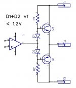
a). What does 'Zener 0V' mean?
b). As soon as D1 starts to conduct, T11 switches on. Will it not fail? (I am afraid that at start of conduction of T11, jointly T11 and T12 will create an inter-rail conduction path, a "short", with no limit to the current, and this could result in failure of these transistors).
c). In this transistor-assisted-Schottky concept, that you are thinking about, would the condition be fulfilled / met, that the Schottky diodes are conducting constantly, all the time? Or would they have periods where the one or the other is inactive? My gut feeling tells me, that the Schottky diodes "should" be conducting all the time, but maybe you see some alternative mechanism, concept, solution here? What is the intent?
===
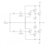
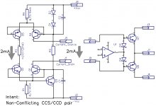
Was thinking about how "not to interfere" with your design goals (resistors, capacitors, et al). Was thinking about how to "force" a constant current flow through the Schottky diodes, irrespective of the fact that they are riding "on the signal", or "floating" on the signal and jumping all around across all possible values ranging from the plus supply rail to the minus supply rail. How do you make a "floating" CCS-CCD pair? I don't know. Not sure. I tried to envision such a "floating CCS-CCD pair" that would be capable of floating on the output of your op-amp, and (possibly/hopefully) not interfering with your circuit too much.
I came up with this stuff. A combination of two series connected CCS (top side) and CCD (bottom side). But in order so as not to antagonize them against each other (so that they do not "fight" against themselves), added a mirror. Result: hopefully a "floating" current source. Probably nonsense. But maybe? Just take a look. Should this floating CCS-CCD be powered from a separate DC power source, or can it be powered from the same Rails as your amplifier? Not sure. The safer bet would be to power it from something separate. But maybe it could also be powered from Your rails. Then You probably would "loose" some 2 volts of your maximum possible output swing. But my bigger concern is that if powered from "Your rails", then there is the risk of various "capacitance" or other problems likely to emerge. Whereas when powered from a totally "separate" power source, there is a higher chance that the floating CCS-CCD would not in any way "interfere" with your low-capacitance Op-Amp concept. Just thinking out loud, fishing for some alternative ideas.
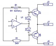
How about conducting a "Simple and Stupid" experiment? Because if no practical value gained, then not worth all the talking. A 9V battery. In series with a 3k9 resistor. Voila! A KISS floating current force. Two Schottky diodes, ... and Rock and Roll. Hopefully.
Attachments
D1 and D2 are to ensure T11 and T21 can be fully closed. Not much of a deal. Zeners can close amplifiers which are away from the rails by more than 0.7V and a better closure of all amplifiers. I wrote Zenners OK. I meant D1 and D2 can be replaced with Zeners.Interesting development. I think that I "feel" where this concept is intended to be going, but I am not sure about some details here. <snip>
Here is the principle :
Assume the amplifier has an output of 0V. Then, T11 and T21 are open and their base resistors ( and collector resistors ) ensure to what extent they are open. Say somewhere in the half of the needed collector current. Exact values are not important. When the output of the amplifier goes high, T11 opens more, T21 closes more. T12 opens more, T22 closes more. T13 can get more current.
T13 and T14 are still governed by the Schotkys and the output of the amplifier. Their bases are 0.35V away from the amplifier. Just the same as resistors.
Of course, precautions must be taken for the currents not to be too high. This can be done by the base and collector (not shown) resistors of T11 and 21.
Need to think more for logic and values. But, generally, I replaced your resistors with transistors which open a lot when the output voltage of the amplifier is very high (or very low). They are opened normally (and, theoretically, equally) when the voltage of amplifier is 0V (in the middle).
I do not have the possibility to look at this schematics closely now, but, looks like you have combined the standard approach of a common emitter transistor and your original circuit. Good think is you tried to replace the resistors with transistors too.Was thinking about how "not to interfere" with your design goals (resistors, capacitors, et al). <snip>
Separate source of the Schottkys is much better. I am still worried of the resistor, though. Your original idea with a current source must be OK.How about conducting a "Simple and Stupid" experiment? <snip>
The Co is necessary. Csi allow for Co to charge and discharge with maximum speed. The external capacitors help Co. They are not necessary but good. Power supply capacitors are good as they are. The more the better.Which speakers do you use? If not multiway, I would remove all the different caps. Would left the biggest only. Currently it sounds like a distorted mirror on the hustle and bustle;-)-; Multiway speakers don't show that.
I would never do use TO-3 transistors.
TO3 transistors are not a problem. 2N3055 and MJ2955 are too powerful for the job which is good because their B is high at 3.375A, but, bad because their parasitic capacitances may be high, although, this may not be true for the new versions. Old 2N3055 and MJ2955 have high parasitic capacitor values. New must have low parasitic capacitor values.
The speakers are normal, general purpose 8 Ohm, 50W, Toshiba tiny speakers. Everything is OK with the capacitors and the speakers. No effect.

Where is the schematic of your amplifier. Are you ashamed of posting it here?
Are you to lazy to click on the link he supplied?

I get the picture shown .Are you to lazy to click on the link he supplied?
Where is the schematic of your amplifier. Are you ashamed of posting it here?
The schematics is in the ADDENDUM of the document as per the link, posted and repeated on many occasions. Here is again : Amplifier – Google Drive
I get the picture shown .
Sorry. Please, read this :
With this post, as well as, with many more, I upload a document on Google Drive and make the folder as well as the document " Public ". Anyone who goes there can download the document. The document contains a lot of explanations, formulae, schematics, etcetera. However, the main schematics is in the Addendum of the document. Addendum is a strange word for the end of the document where information is added. Addendum is a Latin word, but, is used in British English and the root of the word Addendum comes from the English word Add.
Although to add the main schematics is strange, I think the word Addendum means a chapter of the document where specific information is published. Thus, I, usually, publish complete information in the addendum : complete schematic of the device as well as pictures of the device. The rest of the document is explanation and, yes, there are explanation of the complete schematics, published in the addendum, but these are still part of the explanations.
In the explanations section, I, usually try to explain the logic of the electronics and not the mathematical descriptions and formulae unless these are necessary for the explanations, which is seldom the case as electronics is logic and not mathematics. This is why there is a specialty called Electronics Engineering and, another, called Mathematics. Electronics is usually taught in Technical Institutes, whereas Mathematics is taught in real Universities.
However, because of stupidity, some teachers who want to sound scientific and justify their titles and salaries have decided to teach mathematics in Technical Institutes which is a crime against humanity. There is almost no mathematics and whatever there is is very basic and simple and can be figured out in a week or two. Has to be mentioned as a result and not to require theorems to be proven, etcetera in classes of Higher Mathematics.
The biggest stupidity is students of Computer Science are also needed to study mathematics and the only thing they need is to add, subtract, multiply and, occasionally divide. True in binary, mainly and in Hexadecimal, but still.
In Automation theory and control systems, mathematics seems to be necessary, but, this is not true. Only seems. They still use simple end results such as imaginary, filter and system response, etcetera.
In terms of study and use of Mathematics in engineering, I claim to be a specialist, because this is what I have studied for 5 years and, thus, I know how wrong to study mathematics is. The biggest stupidity is to concentrate on integrals which are not used even in integrators.
This is why I strongly fight for electronics, as well as any other engineering, even control systems, without mathematics and only with logic. There are two types of logic : analogue and digital. Analogue logic is more like a process which happens for a give period, although, this period is, usually, accepted to be 0 because electrons travel with a speed of light ( nearly ). However, to accept the period to be 0 is wrong. Thus, even without capacitors and other delays, the current flies slowly with the speed of light and not immediately. Digital logic is self explanatory. There, processes happen immediately as the processes are not part of digital logic but of analogue and, yes, physically, digital systems work in an analogue way, but this is not important. The digital logic they perform is.
In summary : this is why I divide the documents in two :
1. Main Document : Logic : Explanation of the used electronics by logic without mathematics. I try to go as low as possible, such as, how a transistor and a diode work.
2. Addendum : The full schematics and pictures.
Thus,
1. Click here to go to the document : Amplifier – Google Drive
2. Click on the document to download the document to your hard disk or you may just open the document. The best is to use " Save As " and download the document elsewhere, say, on your desktop and, after use, delete the document or move the document wherever you want.
3. The document is written with OpenOffice for obvious reason ( free ), but, should be possible to be viewed with Microsoft Word for Windows 97 and newer. Once the document opens, press Page Down to reach the Addendum. The schematics is first in the Addendum and pictures are second. The schematics, in this case, shows only one of the two stereo channels. The other is identical. Basically, the main components of the simple schematics is one amplifiers, two transistors and one capacitor Co and the cousins of Co, Csi.
You can use the scroll bar, but, you may miss the schematics. Page Down is preferable. There are not so many pages. After each press on Page Down, wait for the page to load fully and include graphics.
In case anyone is interested, because I have the bases of the transistors outside, I may try to put a capacitor from the bases to ground. Such a capacitor is not a good idea because the amplifier will slow down. Anything between the bases and the output of the OA is not welcome and also makes noise.
However, a capacitor with a value 10% of the Ccbe ( the lowest value during the jump ) may be OK and may also reduce Co. The problem is this value of Ccbe is not known and has to be measured. I cannot measure this and can only speculate. LM7171 can drive capacitive loads of 0.5nF without a problem and, probably 1nF and higher. Again Ccbe is not known and the said capacitor is added to Ccbe.
Another good news for LM7171 : I read now and before, the documentation states the open loop outut impedance as 15 Ohms and not 110 as I said in the document. I decided they put a 100 Ohm protection resistor because the maximum current when the output is shunt is 135mA continuously ( the voltage drops to 8V, though ). Looks lie the current protection may not have been done by simple output resistors.
Anyway, 15 Ohms open loop ( saturation ) output impedance of an amplifier sound excellent.
Also, in regards to the LM7171 input limit of 10V pin to pin, 10V is the RMS of 14.1V which is the maximum amplitude of a preamplifier supplied by + - 15V or 30V. Not a very scientific protection, but, for now, I do not need another. LM7171 seems to be very sturdy even without input protection. I have not been able to damage any as far as I remember and I have abused them a lot. However, damage is not the problem. The problem is electronics degrades with the abuse. Thus, an abuse amplifier may seem to be perfectly OK, but, the parameters may have changed after abuse. This is why I replaced them before this version, although, all of them seem to be perfect in terms of parameters too.
And in regards to capacitors and speakers concerns. I do not think 1uF capacitor in parallel of a speaker with a very tiny amount of inductance ( in case any at all ) may affect the performance. The filter would have a huge frequency and, hopefully, no signal can have such.
So far, there have not been any changes of the document after the previous post on the topic of document changes and updates.
- Home
- Amplifiers
- Solid State
- Amplifier