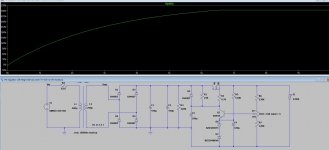
I try simulate 305VDC HV regulate supply adjust by change value of Zener diodes normally 75V zener. To use with 6sn7 and 45 total load is about 86mA
the problem is it take almost 7 seconds to get 305VDC.
How to solve problem?
if anyone can help provide 305vdc HV reg, will be much appreciate
thx
the problem is it take almost 7 seconds to get 305VDC.
How to solve problem?
if anyone can help provide 305vdc HV reg, will be much appreciate
thx
Attachments

2SK3564 of Pspice not compatible to LTspice. How to convert to compatible value? Thank you.
*********************************************************************
* Operation of this model has been verified only on the OrCAD.
*********************************************************************
.SUBCKT NMOS_2SK3564 1 2 3
M0 1 22 3 3 smsmosfet
D1 3 1 DDS2
D2 2 10 DGS1
D3 3 10 DGS2
R2 10 2 1E+009
R3 10 3 1E+009
RG 2 22 13
.MODEL smsmosfet NMOS
*********************************************************************
- (C) Copyright TOSHIBA CORPORATION 2017
- Date: 28/06/2017
- File Name: 2SK3564.lib
- Part Number: 2SK3564
- Parameter Ver.: Ver.1
- Simulator: PSpice
- Model Call Name: NMOS_2SK3564
- TNOM: 25 degree
- Pin Assign: 1=Drain 2=Gate 3=Source
* Operation of this model has been verified only on the OrCAD.
*********************************************************************
.SUBCKT NMOS_2SK3564 1 2 3
M0 1 22 3 3 smsmosfet
- L = 5e-06
- W = 0.03
- AD = 3e-08
- AS = 3e-08
- PD = 0.06
- PS = 0.06
D1 3 1 DDS2
D2 2 10 DGS1
D3 3 10 DGS2
R2 10 2 1E+009
R3 10 3 1E+009
RG 2 22 13
.MODEL smsmosfet NMOS
- LEVEL = 7
- MOBMOD = 1
- CAPMOD = 3
- NOIMOD = 1
- TOX = 1.5e-08
- XJ = 1.5E-007
- NCH = 1.7E+017
- NGATE = 0
- RSH = 0
- TNOM = 25
- VTH0 = 3.3121
- VOFF = -0.08
- NFACTOR = 1.056
- U0 = 1985.7966
- K1 = 0.5
- K2 = 0
- K3 = 80
- K3B = 0
- W0 = 2.5E-006
- NLX = 1.74E-007
- DVT0 = 2.2
- DVT1 = 0.53
- DVT2 = -0.032
- DVT0W = 0
- DVT1W = 5.3E+006
- DVT2W = -0.032
- DWG = 0
- DWB = 0
- UA = 7.3367e-09
- UB = 5.87E-019
- UC = -4.65E-011
- VSAT = 38144.4502
- A0 = 0.28138
- AGS = 7.4506
- B0 = 0
- B1 = 0
- KETA = -0.047
- A1 = 0
- A2 = 1
- DELTA = 9.5046e-05
- RDSW = 93000
- PRWG = 0
- PRWB = 0
- WR = 1
- CDSC = 2.4E-004
- CDSCD = 0
- CDSCB = 0
- CIT = 0
- ETA0 = 0.08
- ETAB = -0.07
- DSUB = 0.56
- PCLM = 1.1514
- PDIBLC1 = 0.39
- PDIBLC2 = 1e-05
- PDIBLCB = 0
- DROUT = 0.56
- PSCBE1 = 4.24E+008
- PSCBE2 = 1E-009
- PVAG = 0
- ALPHA0 = 0
- ALPHA1 = 0
- BETA0 = 30
- NJ = 1
- JS = 0
- XPART = 0
- CGSO = 3.525e-08
- CGDO = 3.7238e-13
- CGBO = 0
- CGDL = 9.9997e-08
- CGSL = 2.5774e-09
- CKAPPA = 0.16384
- CF = 0
- CLC = 1E-007
- CLE = 0.6
- VOFFCV = 0
- NOFF = 1
- DLC = 0
- ACDE = 1
- MOIN = 15
- CJ = 0
- CJSW = 1E-012
- CJSWG = 1E-012
- PB = 1
- PBSW = 1
- PBSWG = 1
- MJ = 0.5
- MJSW = 0.33
- MJSWG = 0.33
- AF = 1
- EF = 1
- KF = 0
- UTE = -1
- KT1 = -2.45
- KT1L = 0
- KT2 = 0.022
- UA1 = 4.31E-009
- UB1 = -7.61E-018
- UC1 = -5.6E-011
- AT = 3500
- PRT = 250000
- XTI = 3
- TCJ = 0
- TPB = 0
- TCJSW = 0
- TPBSW = 0
- TCJSWG = 0
- TPBSWG = 0
- DWC = 0.0082616
- TNOM = 25
- IS = 5.8251e-10
- RS = 0.14804
- N = 1.4
- CJO = 5.3e-10
- VJ = 0.4
- M = 0.59
- XTI = 3
- TT = 1.78e-06
- BV = 900
- IBV = 0.01
- TNOM = 25
- IS = 5.8251e-10
- RS = 0.14804
- N = 1.4
- CJO = 1E-15
- VJ = 0.7
- M = 0.3
- XTI = 3
- TT = 1.78e-06
- TNOM = 25
- IS = 1E-015
- TNOM = 25
- IS = 1E-015
Thank you very much I will change value of R1It takes a long time to charge C3 through R1, the RC timeconstant is 2.4secs. Make R1 much smaller and it will be OK.
Jan
OTOH, a slow rising B+ gives your tube's heaters some time to heat up so it may not be that bad.
Jan
Jan
2SK3564 of Pspice not compatible to LTspice. How to convert to compatible value? Thank you.
*********************************************************************
*
- (C) Copyright TOSHIBA CORPORATION 2017
- Date: 28/06/2017
- File Name: 2SK3564.lib
- Part Number: 2SK3564
- Parameter Ver.: Ver.1
- Simulator: PSpice
- Model Call Name: NMOS_2SK3564
- TNOM: 25 degree
- Pin Assign: 1=Drain 2=Gate 3=Source
* Operation of this model has been verified only on the OrCAD.
*********************************************************************
.SUBCKT NMOS_2SK3564 1 2 3
M0 1 22 3 3 smsmosfet
D0 3 1 DDS1
- L = 5e-06
- W = 0.03
- AD = 3e-08
- AS = 3e-08
- PD = 0.06
- PS = 0.06
D1 3 1 DDS2
D2 2 10 DGS1
D3 3 10 DGS2
R2 10 2 1E+009
R3 10 3 1E+009
RG 2 22 13
.MODEL smsmosfet NMOS
.MODEL DDS1 D
- LEVEL = 7
- MOBMOD = 1
- CAPMOD = 3
- NOIMOD = 1
- TOX = 1.5e-08
- XJ = 1.5E-007
- NCH = 1.7E+017
- NGATE = 0
- RSH = 0
- TNOM = 25
- VTH0 = 3.3121
- VOFF = -0.08
- NFACTOR = 1.056
- U0 = 1985.7966
- K1 = 0.5
- K2 = 0
- K3 = 80
- K3B = 0
- W0 = 2.5E-006
- NLX = 1.74E-007
- DVT0 = 2.2
- DVT1 = 0.53
- DVT2 = -0.032
- DVT0W = 0
- DVT1W = 5.3E+006
- DVT2W = -0.032
- DWG = 0
- DWB = 0
- UA = 7.3367e-09
- UB = 5.87E-019
- UC = -4.65E-011
- VSAT = 38144.4502
- A0 = 0.28138
- AGS = 7.4506
- B0 = 0
- B1 = 0
- KETA = -0.047
- A1 = 0
- A2 = 1
- DELTA = 9.5046e-05
- RDSW = 93000
- PRWG = 0
- PRWB = 0
- WR = 1
- CDSC = 2.4E-004
- CDSCD = 0
- CDSCB = 0
- CIT = 0
- ETA0 = 0.08
- ETAB = -0.07
- DSUB = 0.56
- PCLM = 1.1514
- PDIBLC1 = 0.39
- PDIBLC2 = 1e-05
- PDIBLCB = 0
- DROUT = 0.56
- PSCBE1 = 4.24E+008
- PSCBE2 = 1E-009
- PVAG = 0
- ALPHA0 = 0
- ALPHA1 = 0
- BETA0 = 30
- NJ = 1
- JS = 0
- XPART = 0
- CGSO = 3.525e-08
- CGDO = 3.7238e-13
- CGBO = 0
- CGDL = 9.9997e-08
- CGSL = 2.5774e-09
- CKAPPA = 0.16384
- CF = 0
- CLC = 1E-007
- CLE = 0.6
- VOFFCV = 0
- NOFF = 1
- DLC = 0
- ACDE = 1
- MOIN = 15
- CJ = 0
- CJSW = 1E-012
- CJSWG = 1E-012
- PB = 1
- PBSW = 1
- PBSWG = 1
- MJ = 0.5
- MJSW = 0.33
- MJSWG = 0.33
- AF = 1
- EF = 1
- KF = 0
- UTE = -1
- KT1 = -2.45
- KT1L = 0
- KT2 = 0.022
- UA1 = 4.31E-009
- UB1 = -7.61E-018
- UC1 = -5.6E-011
- AT = 3500
- PRT = 250000
- XTI = 3
- TCJ = 0
- TPB = 0
- TCJSW = 0
- TPBSW = 0
- TCJSWG = 0
- TPBSWG = 0
- DWC = 0.0082616
.MODEL DDS2 D
- TNOM = 25
- IS = 5.8251e-10
- RS = 0.14804
- N = 1.4
- CJO = 5.3e-10
- VJ = 0.4
- M = 0.59
- XTI = 3
- TT = 1.78e-06
- BV = 900
- IBV = 0.01
.MODEL DGS1 D
- TNOM = 25
- IS = 5.8251e-10
- RS = 0.14804
- N = 1.4
- CJO = 1E-15
- VJ = 0.7
- M = 0.3
- XTI = 3
- TT = 1.78e-06
.MODEL DGS2 D
- TNOM = 25
- IS = 1E-015
.ENDS
- TNOM = 25
- IS = 1E-015
psice is happy with "+" being used to split models on lines but I found that never works for LTSpice so I reformat:
Code:
.SUBCKT NMOS_2SK3564 1 2 3 M0 1 22 3 3 smsmosfet L=5e-6 W=0.03 AD=3e-8 AS=3e-8 PD=0.06 PS=0.06
D0 3 1 DDS1
D1 3 1 DDS2
D2 2 10 DGS1
D3 3 10 DGS2
R2 10 2 1E+9
R3 10 3 1E+9
RG 2 22 13

.MODEL smsmosfet NMOS LEVEL=7 ... do the same here for all bulleted (with a "+")
.MODEL DDS1 D ... again here.
.MODEL DDS2 D ... again..
.MODEL DGS1 D TNOM=25 IS=1E-15
.MODEL DGS2 D TNOM=25 IS=1E-15
.ENDS
Leave the Dn and Rn etc on separate lines as I've shown above. It may be that LTSpice doesn't like the LEVEL=7 command, it's been a while since I did any LTSpice model programming.
I see the SK3564 datasheet doesn't have SOA chart which is a bit concerning. The DC operation at HV will lower the current capacity then typically they need derating with temperature. None of that information is in the SK3564 datasheet which may prove a limit that doesn't exist in LTSpice. You could use key+mouse click on the component to get a wattage graph instead of voltage. I don't know that on the PC as I used the Fn key on the Mac.
EDIT: also LTSpice may not like the e+009 or e+08 instead I've reformatted to e+9 etc in above.
Oh thank you then how many seconds are appropriateOTOH, a slow rising B+ gives your tube's heaters some time to heat up so it may not be that bad.
Jan
thank you in advanced
Thank you so much i will trypsice is happy with "+" being used to split models on lines but I found that never works for LTSpice so I reformat:
Code:.SUBCKT NMOS_2SK3564 1 2 3 M0 1 22 3 3 smsmosfet L=5e-06 W=0.03 AD=3e-08 AS=3e-08 PD=0.06 PS=0.06 D0 3 1 DDS1 D1 3 1 DDS2 D2 2 10 DGS1 D3 3 10 DGS2 R2 10 2 1E+9 R3 10 3 1E+9 RG 2 22 13 .MODEL smsmosfet NMOS LEVEL=7 ... do the same here for all bulleted (with a "+") .MODEL DDS1 D ... again here. .MODEL DDS2 D ... again.. .MODEL DGS1 D TNOM=25 IS=1E-015 .MODEL DGS2 D TNOM=25 IS=1E-015 .ENDS
Leave the Dn and Rn etc on separate lines as I've shown above. It may be that LTSpice doesn't like the LEVEL=7 command, it's been a while since I did any LTSpice model programming.
I see the SK3564 datasheet doesn't have SOA chart which is a bit concerning. The DC operation at HV will lower the current capacity then typically they need derating with temperature. None of that information is in the SK3564 datasheet which may prove a limit that doesn't exist in LTSpice. You could use key+mouse click on the component to get a wattage graph instead of voltage. I don't know that on the PC as I used the Fn key on the Mac.
EDIT: also LTSpice may not like the e009 instead I've updated to e9 in above.
I've just made an update/comment on the reformatting of leading zeros in the e+009 etc if, after the new line reformat, that doesn't work try the e reformat. If you look at the log (the Mac it's ctrl+L iirc) you'll see any issues the parser had at the top. I've had LEVEL issues before - that is more involved and it's easier to search for a new compatible model than play with the parameters and end up with a bad model.Thank you so much i will try
Maybe 7 secs isn't so bad. Where does the schematic come from, is it an existing design?Oh thank you then how many seconds are appropriate
thank you in advanced
Jan
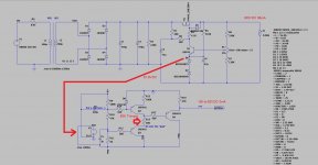
You should split R1 and connect C3 to the junction of the 12K's, otherwise the active regulation is neutralized in AC
Can you help draw rough picture? Thank youYou should split R1 and connect C3 to the junction of the 12K's, otherwise the active regulation is neutralized in AC

Also want a gate protection diode across the mosfet source to gate to prevent it going positive should the caps discharge at different rates.
If you want a belt and braces a 1007 across the drain-source to prevent reverse polarity and not rely on the internal diode..
How does C3 bleed? (R1+R3 I assume)
If you want a belt and braces a 1007 across the drain-source to prevent reverse polarity and not rely on the internal diode..
How does C3 bleed? (R1+R3 I assume)
Here it is:

And while you are at it, you could add a protection zener too. On the other hand, I do not clearly see the purpose of D5
And while you are at it, you could add a protection zener too. On the other hand, I do not clearly see the purpose of D5
Here it is:
View attachment 1082227
And while you are at it, you could add a protection zener too. On the other hand, I do not clearly see the purpose of D5
It prevents current bypassing the mosfet but allows bleed of C3 on startup shutdown?
Thank you very muchHere it is:
View attachment 1082227
And while you are at it, you could add a protection zener too. On the other hand, I do not clearly see the purpose of D5
- Home
- Amplifiers
- Power Supplies
- 305Vdc HV regulator adjustable via zener diode too slow 7seconds