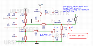
The important thing is that electrolytic capacitors are caught in a negative feedback loop.I would like to note that the selected gain is relatively small - only 4 times. As a result, the amplifier has deep negative feedback, which reduces distortion. It is not difficult to obtain the required preamplifier gain up to a voltage of Udd/4 Vpp.
Capacitor C32 is of great importance for quality, because it determines the linearity of the Q17 amplification. It is simply selected with a large nominal value for C32 (470 μF) and R79 (100 R), the time constant will be 47 mS, which is not small.The final amplifier circuit uses a capacitance of 2000 µF and works on a speaker system with an impedance of 6 ohms..
C35 equal to 2000 μF - is good.
For speaker systems this is not noticeable; for headphones it can be less, if you wish.A quick simulation shows that with a capacitance of the output coupling capacitor of 4700 μF and an 8-ohm load at a frequency of 20 Hz, the phase shift will be 11 degrees
I think it might be interesting using a MOSFET LTP input, changing to dual rail and removing C35. this would only cost another transistor but may sacrifice some stability 🤔
To be fair the design how it is with less than 0.1% distortion is good for such a simple design. beauty in the simplicity
To be fair the design how it is with less than 0.1% distortion is good for such a simple design. beauty in the simplicity
Of course, you can complicate the circuit design and get some improvement in parameters, but is it worth it? There are already a lot of very complex amplifier circuits on this forum 🙂
I see further development of this scheme in a different direction. The use of Schottky diodes and current stabilization allows the amplifier to operate effectively in a mixed class AB. Of course, when the amplifier operates in class A, this is more preferable due to low distortion and short spectrum, but the amplifier consumes more power. The idea is to increase the quiescent current of the output transistors depending on the volume of the output signal. That is, when we listen to music at low volume (2-3W), it will be enough for us to set the quiescent current to a small one, for example 200-300mA. This will be enough for the amplifier to operate in class A. As the volume increases, the quiescent current should increase, for example, to 1A. I don’t yet see obvious solutions to how to do this simple, but it will be interesting to think about it.
I see further development of this scheme in a different direction. The use of Schottky diodes and current stabilization allows the amplifier to operate effectively in a mixed class AB. Of course, when the amplifier operates in class A, this is more preferable due to low distortion and short spectrum, but the amplifier consumes more power. The idea is to increase the quiescent current of the output transistors depending on the volume of the output signal. That is, when we listen to music at low volume (2-3W), it will be enough for us to set the quiescent current to a small one, for example 200-300mA. This will be enough for the amplifier to operate in class A. As the volume increases, the quiescent current should increase, for example, to 1A. I don’t yet see obvious solutions to how to do this simple, but it will be interesting to think about it.
yes, I see exactly what you mean, agreed. focusing on the output stage would be the way to go. maybe a current sense resistor in line with the speaker load feeding back to Q16?
I'm going to have to think about it. 👍
I'm going to have to think about it. 👍
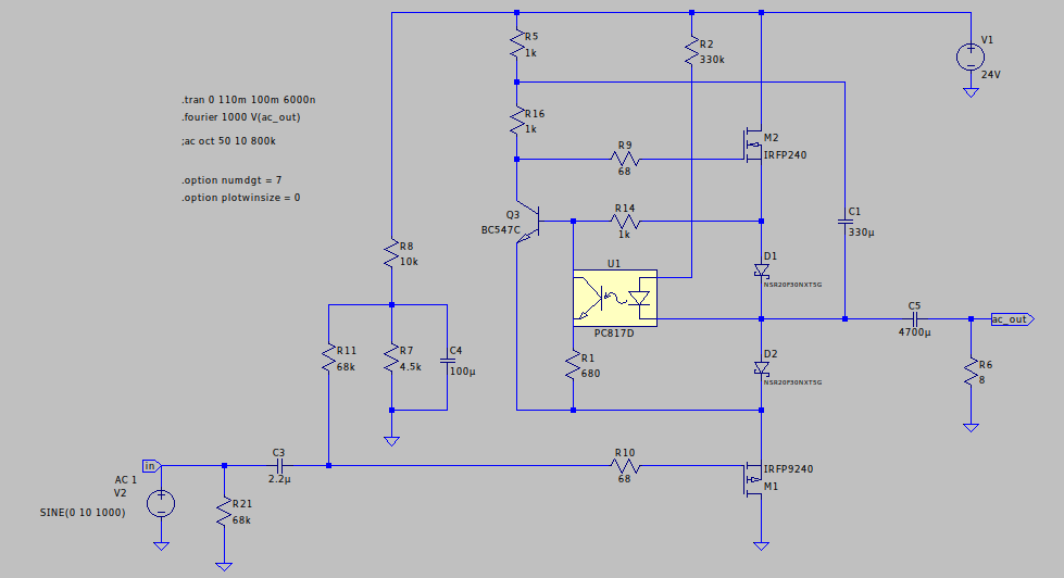
Yeah its definitely not obvious :/ I thought I had something promising using an optocoupler, but needs more work.
If I understand the problem correctly you need to increase the current only on the negative half of the waveform?
If I understand the problem correctly you need to increase the current only on the negative half of the waveform?
ur5ffr,
Over the years, Krell has played around quite a bit with some of what you mentioned.
In case it might give you food for thought, you can start to read about some of that here: https://tmraudio.com/blog/krell-class-a-all-the-way/
Over the years, Krell has played around quite a bit with some of what you mentioned.
In case it might give you food for thought, you can start to read about some of that here: https://tmraudio.com/blog/krell-class-a-all-the-way/
I see one possible solution like this:Yeah its definitely not obvious :/ I thought I had something promising using an optocoupler, but needs more work.
This circuit works like this: as the output signal increases, the resistance of the photoresistor OR1 decreases. This causes an increase in current through U7 which stabilizes the stage at transistor Q7. This is essentially positive feedback. It should be very inertial (slow). And here we have the danger of overshoot, which will lead to an unacceptably strong increase in the quiescent current. In addition, the photoresistor can introduce unwanted distortions. Therefore, this is just an idea that requires clarification.
UR5FFR so how much of a time delay for a higher/lower quiescent current are you thinking? I was honestly thinking of simply replacing R12 with an NTC thermistor mounted on the heat sink, thus allowing for the maximum current permitted by temperature.
I have been experimenting with your design and and have found an emitter follower driving the lower FET helps a lot with distortion and the value of the first collector resistor can be increased.
Here is what I have setup:
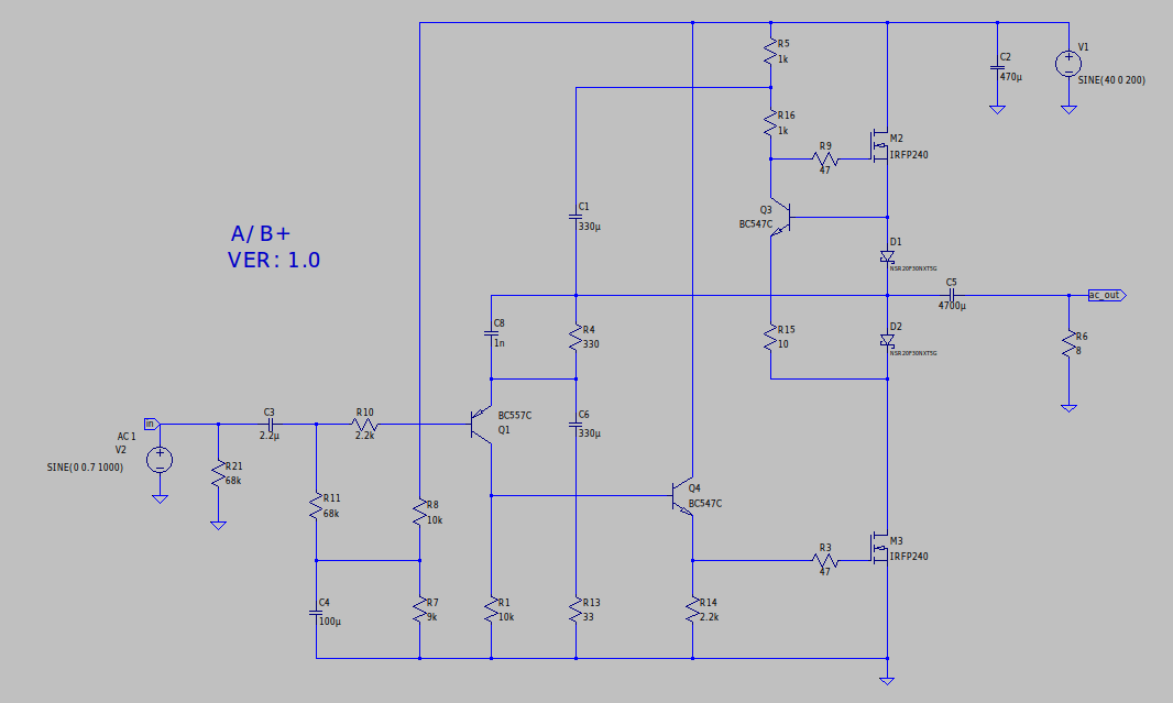
C8 was necessary to prevent oscillation- though no zobel network was needed.
Yes, C6 could do with being a higher value to prevent low freq roll off.
Quiescent current is 300ma. Gain has been increased.
Here's the distortion profile just before clipping (23v p-p) into 8ohm load:
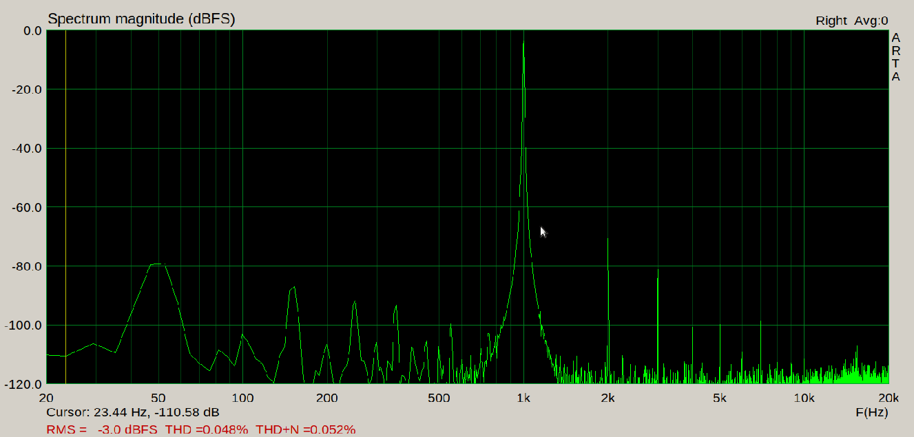
I think this is a very good result, and don't mind the 50hz mains interference I don't have the best test setup 😆
Another note is distortion stays very similar over frequency and does not increase much at all at higher frequency's like one would expect.
I have been experimenting with your design and and have found an emitter follower driving the lower FET helps a lot with distortion and the value of the first collector resistor can be increased.
Here is what I have setup:
C8 was necessary to prevent oscillation- though no zobel network was needed.
Yes, C6 could do with being a higher value to prevent low freq roll off.
Quiescent current is 300ma. Gain has been increased.
Here's the distortion profile just before clipping (23v p-p) into 8ohm load:
I think this is a very good result, and don't mind the 50hz mains interference I don't have the best test setup 😆
Another note is distortion stays very similar over frequency and does not increase much at all at higher frequency's like one would expect.
Last edited:
I think that positive temperature feedback is a bad solution. It can lead to uncontrolled heating of the output transistors.UR5FFR so how much of a time delay for a higher/lower quiescent current are you thinking? I was honestly thinking of simply replacing R12 with an NTC thermistor mounted on the heat sink, thus allowing for the maximum current permitted by temperature.
You did a good job! But you can improve it. I would recommend reducing the resistance of resistors R5R16R14 by two to three times. This affects the increase in distortion with increasing frequency, since through them the gate capacitance M2 is charged. I applied a rectangular signal to the input and observed its shape at the output. Large values of these resistors lead to deterioration of the edges of the square wave signal.I think this is a very good result
Another significant point is the ratio of resistors R4R13. It sets the gain, but also affects the distortion. High gain means high distortion. Therefore, in my circuit I set the gain to 4 times. This also led to a reduction in distortion.
You can also play with the quiescent current. Increasing it leads to a decrease in distortion.
Although I am testing with 24v I do plan on running at around 30-40v in the final build, thus the gain is set higher as well as R5 R16 R14 being a higher value and running at 300ma to manage heat dissipation, especially in R4 R5. I will test and try lowering the values though.
I did some square wave tests and saw a fast rise and fall time, didn't seem a problem.
I did some square wave tests and saw a fast rise and fall time, didn't seem a problem.
So what was your power supply design? how much capacitance and ripple? any hum problems?
Also do you have any pictures of the inside out of interest 🤔
Also do you have any pictures of the inside out of interest 🤔
I use a switching power supply without a voltage stabilizer. It produces 30V without load. With a load of 2A, the voltage drops to 28V.
I used 10000uF in the power filter and don't see any problems with hum.
I used 10000uF in the power filter and don't see any problems with hum.
I was referring to an NTC thermistor (resistance falls as temperature rises) if placed in parallel with R12 (on your circuit post #29) then I think it would be negative temperature feedback meaning as temperature rises, the current will be lowered. you could select the correct starting resistance for the thermistor (and R12 value) for maximum current wanted, and can only be lowered meaning it would 'make the most' of the heatsink and keep a constant temperature. its just a thought.I think that positive temperature feedback is a bad solution. It can lead to uncontrolled heating of the output transistors.
Last edited:
Hello,
Thank you for your work.
I tried your circuit (class AB with 4.7/10 ohm and diodes) on a breadboard and it works very good with little noise. However, when I try to sold the components onto a prototype board, the power of the MOSFETs rocket to over 100 W and cannot be used (you can imagine the heat generated). I've checked the connections many times and found no error at all. I have another class AB amplifier circuit using MOSFETs IRF540/9540 and had exactly the same problem. It seems that MOSFETs can only work on printed PCB but not prototype board.
Could you share the PCB layout? Thank you.
Hi
?
what do you mean with
It seems that MOSFETs can only work on printed PCB but not prototype board.
did you use a heat sink?
kr
chris
?
what do you mean with
It seems that MOSFETs can only work on printed PCB but not prototype board.
did you use a heat sink?
kr
chris
I use heat sinks for both arrangements.
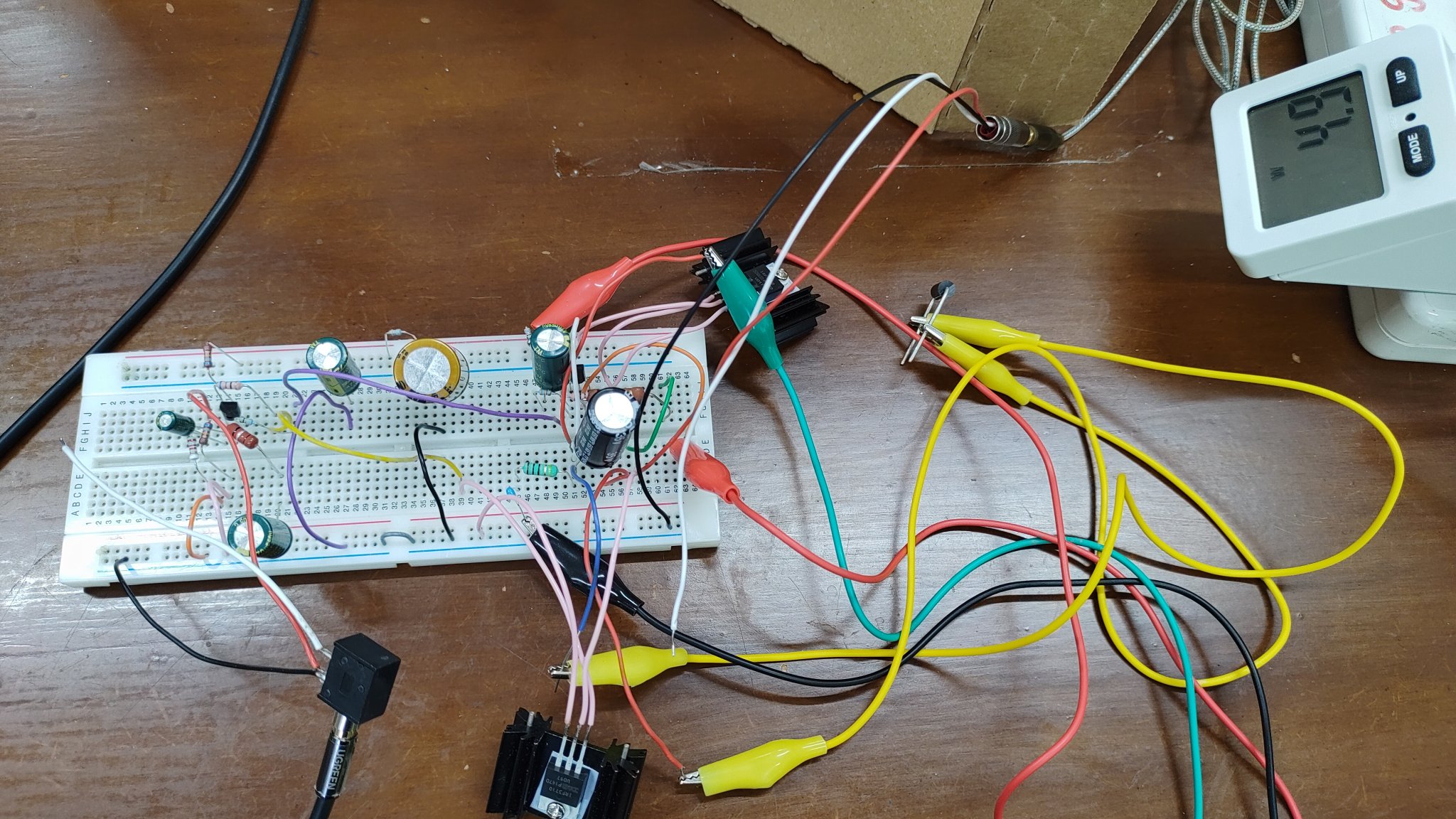
The above is on a breadboard. It works perfectly and the power is about 3 W as indicated (the 24V power supply consumes 2W). The MOSFETs are at about 40C.
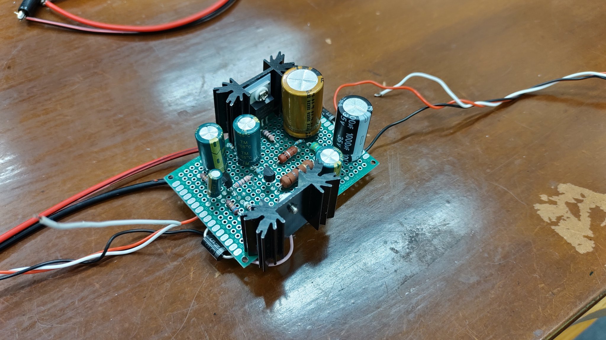
The above does not work. The power rise to over 100 W and cause overheating. I've checked the circuit many times and found error.
The above is on a breadboard. It works perfectly and the power is about 3 W as indicated (the 24V power supply consumes 2W). The MOSFETs are at about 40C.
The above does not work. The power rise to over 100 W and cause overheating. I've checked the circuit many times and found error.
- Home
- Amplifiers
- Solid State
- Very simple MOSFET design in class A/A+/B
