Hi ! i am just a beginner and please be free to move this thread to a more proper location 
i have a question about bjts buffers
Is it possible to get low THD buffer from very basic discrete circuits ?
I am attaching an example of what i mean
I am noticing that using a npn and a pnp together instead of using just one bjt as a common collector there is a sort of THD cancellation ?
Is this a general effect ?
I have already a schematic of a decently low THD buffer ... if i add another branch mirroring it (i.e. replacing npn with pnp and viceversa) could i get even lower THD ?
Thank you very much to All
gino
Attachments
Last edited:
Hi thank you for the very kind advice Is there a schematic indicating the Voltage at the Q100 fet gate ?
i have discovered lately LTSpice and i am getting the THD attached
I wonder if with a better resistors choice i could get even a lower THD
i have discovered lately LTSpice and i am getting the THD attached
I wonder if with a better resistors choice i could get even a lower THD
Attachments
Last edited:
Thank you very much indeed Mr Mooly Your settings have been a God send to me !
I hope one day i will be able to understand what they really mean But they work just great
Now i am playing with the SW all the day checking schematic taken from service manuals
I see that the buffer can work also with 18VDC incidentally the voltage of many laptop power supplies I guess that some filtering could be needed
However speaking of the simulation i have already checked that some famous basic preamps of the past are not so special at least in terms of THD
I have already been advised many times that if very low THD is the goal nothing beats the tiny opamps
However judging from THD spectrum this essential buffer should impart a nice warm to the sound I intend to build one very soon
Thank you very much again for your kindness and valuable help
Kind regards
gino
Attachments
Last edited:
The B1 is not going to beat a CFP on THD with a significant load (and it's not 2 BJT).
Apart from the CFP, Steve's proposition of a PP buffer is probably the most sensible but bias will be an obstacle.
Unfortunately the CFP doesn't rely on cancellation for the low THD: all of the parasitic effects like Early effect and non-linearity of the BE junction work in the same direction. The good performance is down to the total feedback around the two transistors.
Another option would be the complementary replicator circuit (a kind of half-diamond), but I don't think it will beat the CFP, although it offers some cancellation
Hi thank you very much for your valuable advice Actually i have seen nice results from sim for CFP buffers ( I use a load of 5kohm Quite low for any power amp Should i add 1nF maybe ?)
I cannot get low THD if i want gain from CFP I guess there is a technical reason that i dont know I was thinking that an old CFP was very fine but after sim it the THD is not that low at all
I have tried another buffer stacking one npn above the other (like the Nelson Pass i mean) and the result looks interesting
I am sure it could be refined even more by an expert designer
Attachments
I see that the buffer can work also with 18VDC incidentally the voltage of many laptop power supplies I guess that some filtering could be needed
Switching supplies are not always the best option for low level signal circuitry unless you can filter the output properly and that can be a more difficult than you might think. In practice physical layout of how filter parts connect together are critical.
Good morning yes smps can be quite noisy Nevertheless i have seen SMPS of good grade used in expensive equipment MeanWell is a great brand
As you say filtering can be challenging But the convenience of a smps is intriguing And DC-DC converters are even more convenient
I am intrigued by power supplies even more than audio circuits I enjoy the sound of silence a lot
As you say filtering can be challenging But the convenience of a smps is intriguing And DC-DC converters are even more convenient
I am intrigued by power supplies even more than audio circuits I enjoy the sound of silence a lot
Meanwell are very good but all SMPS has some noise on the output. You can attempt to simulate this by adding a spiky HF content to the supply.
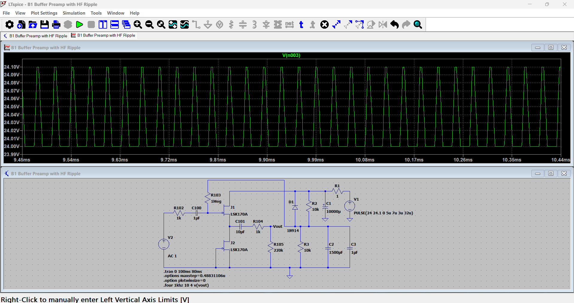
Set the input voltage to zero and look at the amp output to see what is there. A real build would be different but this gives an idea. This is the output voltage of the amp. The rail ripple is just 100mv peak to peak here. For any filtering caps you should use proper models where more than just the capacitance is modelled such as here (for C1). I should have done the same for C2 and C3 but didn't
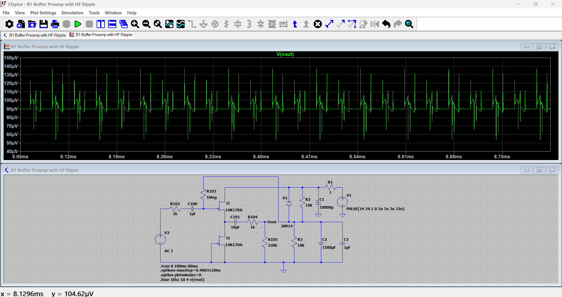
Attached sim has them correctly modelled.
Set the input voltage to zero and look at the amp output to see what is there. A real build would be different but this gives an idea. This is the output voltage of the amp. The rail ripple is just 100mv peak to peak here. For any filtering caps you should use proper models where more than just the capacitance is modelled such as here (for C1). I should have done the same for C2 and C3 but didn't
Attached sim has them correctly modelled.
Attachments
Good morning Mr Mooly Your posts are extremely welcomed and appreciated I have found what to do this summer 
I have just retired from my job and i am having great time after you showed me how to use the sim SW for basic simulations
I have already seen that some old equipment very praised are not so exceptional at least at sim
I need time to elaborate all the information you kindly provided to me
I promise i will study on this topic with effort I love power supplies
Just one kind further advice on a nice power supply i would like to check File attached
Is there a way to see the VDC out and the residual ripple at the output ? i think i have missed something ... the sim does not run
Do i have to put an AC transformer at the input ?
Attachments
Last edited:
Mark Tillotson explained it in the other threadI cannot get low THD if i want gain from CFP I guess there is a technical reason that i dont know
many similar buffers are described in the national semi app note on the LH0033 buffer: ti SNOA725A or app note 227, 1oct 1979.
Jfet followers need a highZ load for low THD, so a BJT buffer helps out. I had good results with a PNP gain stagedriving a complementary follower and a cascoded Jfet input stage fed back to unity gain. for noise the Jfet low output impedance shorted the noise of the buffer and amplification stage, so a very large DR was achieved.
Jfet followers need a highZ load for low THD, so a BJT buffer helps out. I had good results with a PNP gain stagedriving a complementary follower and a cascoded Jfet input stage fed back to unity gain. for noise the Jfet low output impedance shorted the noise of the buffer and amplification stage, so a very large DR was achieved.
Hi yes i remember Still there is idea of pushing CFP limits in my mindMark Tillotson explained it in the other thread
seriously i wonder how low THD can get with the proper selection of best parts, working points, supply voltage ... do not you see the challenge ?
Just one kind further advice on a nice power supply i would like to check File attached
Is there a way to see the VDC out and the residual ripple at the output ? i think i have missed something ... the sim does not run
Do i have to put an AC transformer at the input ?
Delete all the unattached items.
You do not need the timestep and .four commands for this.
Run the sim for much longer, say 10 seconds.
D2, D4 and C2 are not connected.
Remember the AC input voltage is a peak value. So 12 volts in the sim settings is 8.4 volts rms.
Set the sim to run for say 30 seconds and to start saving data at say 29.4 seconds to see the ripple.
Attachments
Hi and thank you sincerely again. I understand that i should have studied first the manual I will do I will start from power supplies
I understand that chip regulators have usually poor PSRR above certain frequencies
The idea is to use some discrete pre-regulators before usual fixed regulators I will not go above +/-24VDC
I followed also a very interesting thread on capacitance multiplier I think that active filtering should be more efficient than passive filtering
Nevertheless i hope to be able in the near future to sim also some passive LC or RC filters
If i had discovered this SW long ago my approach to audio would have been more rational it's never too late
Thank you very much indeed
Any normal active regulator will have a worsening PSRR as frequency increases. L/C or a combination of L/C and R/C is the way to go for removing the sort of noise you get from SMPS. For normal mains transformer type supplies active regulators perform really well as the ripple and noise is low frequency.I understand that chip regulators have usually poor PSRR above certain frequencies
For something unique, at least in my experience, here are two discrete JFET buffer circuits. Both utilize an N-type, dual-JFET device. In this case, a small 2SK2145. Although, it should also work with any other dual-JFET, such as the LSK489. I first saw these two circuits in a recent electronics magazine article, and had never seen them before. Each buffer appears familiar, but only on first glance. One buffer appears to be a typical B1 type totem-pole, and the other appears to be a typical ‘White’ cathode follower type, with a familiar adaption to JFETs.
Upon closer inspection, something unusual becomes apparent. The JFET Sources are connected together. A connection which is not optional with the 2SK2145, as they are tied together internally, by the way. The upper JFET’s Source is connected to the buffer output, as expected, but the lower JFET’s Source is also connected to the buffer output, even though both are N-types. The lower FET’s Drain is connected to the negative supply rail. Essentially, the lower FET appears connected in inversion. For some reason, this configuration seems to greatly linearize the buffer, at least, into 600 Ohms. I presume the test frequency is 1kHz, although I didn’t see that specified in the article. Here are some basic performance figures given in the article. Keep in mind that these are two-transistor, open-loop buffers.
1) THD of the B1 totem-pole topology buffer: 0.07% @ 18Vpk-pk, into 600 Ohms.
2) THD of the White follower topology buffer: 0.006% @ 19Vpk-pk, into 600 Ohms.
That performance stated in the magazine article is what first caught my eye. I would simply have presumed they were typical two-transistor buffer designs, and passed them by. I can’t verify the performance numbers given in the article, because I haven’t built and measured the circuits for myself. So, I’m not yet sure I believe them. If anyone does build and measure them, please share your results with the thread.
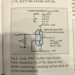
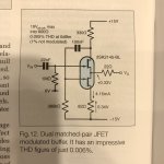


it is the old lh0033 first stage schematic. both fets are operated in the idss mode, the lower one acting as current source load for the follower. indeed drain and source can be swopped. with matched fets and symmetrical voltages bothinput fets operate under the same conditions and offset should be minimal, operation at zero Vgs.
- Home
- Source & Line
- Analog Line Level
- Kind request of help _ basic but low THD discrete buffers


