And this is the more evolved, 154dB@100Hz variant. Some work will be necessary on the two compensation capacitors. Note that not all the protection components have to be present in all situations; depending on the context, some might be dispensed with (and it applies to the two variants), but as drawn they should be reasonably bullet-proof.

Attachments

A looking at stability, switching V1 to DC 420V and hanging an AC1 current, I1 on the output (with 25mA DC load). This graph is from 10kHz to 10MHz. Looks pretty stable to me. (This is the non-invasive analysis method from Omicron-Lab, https://www.omicron-lab.com/applica...tional-and-non-invasive-stability-measurement )
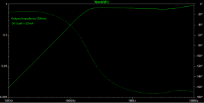
The impedance troughs around 10 microOhms at ~100Hz which is impressive.
The impedance troughs around 10 microOhms at ~100Hz which is impressive.
Attachments
Or a CCS (JFET) in the place of the resistor R5. [I did that with following Darlington. Initially also intended as slow-start-up...] - I'm late to the party I see. I was asleep for a long time. Really.Why no Zener diode at the base of Q1? It will increase mains ripple rejection ("PSRR at low frequencies") by many decibels.
Am I wrong or there's a slight displacement to the left and up, to the impedance curve in LTSpice after these changes are made to the original Diego's regulator? Psrr is not affected, and noise we can't get reliable results of.I have used a Dienoiser in the sensitive section of a frequency synthesizer, and I noticed that for 6V the values from the table published by Diego are not optimal.
This is the modified circuit:
View attachment 1295143
With the original values, the the Vce of Q1 was <1V, which is not very healthy: the transistor works in quasi-saturation mode, and the possible correction amplitude is limited.
With R3 at 470 ohm instead of 1K2 and R5 connected differently, the collector voltage is more reasonable, and the current through Q1 is higher, which is beneficial for the noise performance
Attachments

Couldn't agree more, and I know there's nothing catastrophic in it. Diego always said that his circuit needed specific adjustments, slight ones, to make it work as it should. The long time since I don't use LTSpice and my failing memory on electronic matters made me forget how to simulate impedance in ohms. Could you refresh it?
I managed to design and order full SMD single and dual boards. They have alternative LED footprints on the backside and can be configured LC/RC or fuse and C input.
Should work for 5-30Vout. SOT223 package is rated for 1W so 200-300mA should be fine.
Need to order some parts for testing, hope I can find the stubby output caps (35V rating). Else they'll be a bit taller. And I also need to test them, final design might change a bit.
Should work for 5-30Vout. SOT223 package is rated for 1W so 200-300mA should be fine.
Need to order some parts for testing, hope I can find the stubby output caps (35V rating). Else they'll be a bit taller. And I also need to test them, final design might change a bit.
Attachments


You're a little too tight on clearance towards the board edge at the output connectors. The traces are pretty flimsy to begin with (beef them up to 25-50mil if space allows), and the one on the smaller board already looks damaged on the photo. Better find another way to route them away from the board edges in your next revision - and allow some more space to make them wider.
- Home
- Amplifiers
- Power Supplies
- D-Noizator: a magic active noise canceller to retrofit & upgrade any 317-based V.Reg.