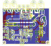
Ignoring the silk that needs tidying. This is the proposed layout that will go to print mid next week.
Kindly make comments especially WSJ, Evette etc
The layout looks good, however, there are a few areas of concern.
The base of Q8 is the amplifier summing junction, with an openloop gain >1,500 (64db) the design goal is to place all components close together and keep this trace as short as possible. R22 could be moved up and C8 moved down to shorten the summing junction trace and reduce the coupling between Q8 base and collector. The trace connected to Q8 collector is connected to the negative supply, which crosses the summing junction trace and is therefore capacitive coupled to the summing junction. Move Q8 collector trace away form the summing junction. Look at all AC signal sources near the summing junction as a capacitively coupled noise source to the summing junction.
I would add a 30 pF cap between Q12 base and collector and measure the phase margin without C4, C11, C9 or C5. I don't see the benefit of R25 or R26.
I would use a single connector for +/- power, power gnd, and speaker connections or at least dual holes for male disconnect terminals, Keystone 1287.
OnAudio,
Good work.
A few comments:
R15 and C7 (100 Ohms, 470 pF) look like a lowpass filter for the input, probably for RF. That's a very good idea but the cutoff frequency is kind of high, at 3.4 MHz. I think it would be better to put it at about 1/10th of that. So I'd probably increase the 470 pF to 4700 pF or so.
Regarding the two 33uF caps for the power supply inputs: This might not be overly important, but having them off to the side is not really the best way. The pads for the pins of caps that go in the power trace should be downstream from the power input, and should be situated so that the power rail current must all pass directly through the capacitor's pad, on its way to or from the loads. Usually, if the trace is wider than the cap's pad, it should even be narrowed, at that point, to be no wider than the pad, so that the current must go very near the cap's lead, as it flows past.
R31 seems to be overlapping three other components.
There are quite a few acute angles (i.e. less than 90 degrees), in the top half. Those are known as "acid traps" in the pcb fab industry. There should be no acute angles.
I would probably fill the area around the output trace with the power rail copper, to minimize the enclosed loop area, so it won't radiate so much. Or maybe ground, whatever makes more sense as far as keeping current in and current out close together.
I think that it is risky to not have much more capacitance, much closer to the output transistors. There should also be high-frequency bypass caps, no?
I would also want the 68pF caps (and everything else) to connect very close to the bases, and would want ground plane for all traces to bases (especially signal traces). Otherwise, they are hum and noise and RF antennas.
Since you have another layer that seems underutilized, think about where the currents go, and then how they come back. Those two should never, ever be separated. Otherwise it makes either a transmitting or receiving antenna. (See Faraday's Law.)
All of WSJ's comments should be implemented, too. He's much better at these types of amplifiers than I am. I hope that he will correct anything I have said that is wrong, or not important.
Cheers,
Tom
Thank you. Highly appreciated.
")
Will check whether I have the model.
Thank you WSJ.
To be doneThe layout looks good, however, there are a few areas of concern.
The base of Q8 is the amplifier summing junction, with an openloop gain >1,500 (64db) the design goal is to place all components close together and keep this trace as short as possible. R22 could be moved up and C8 moved down to shorten the summing junction trace and reduce the coupling between Q8 base and collector. The trace connected to Q8 collector is connected to the negative supply, which crosses the summing junction trace and is therefore capacitive coupled to the summing junction. Move Q8 collector trace away form the summing junction. Look at all AC signal sources near the summing junction as a capacitively coupled noise source to the summing junction.
The schematic is extracted from a model using the 'formula' it works well as is. I hope in time with listening tests the role of R25 and R26 will be appreciated or disapproved.I would add a 30 pF cap between Q12 base and collector and measure the phase margin without C4, C11, C9 or C5. I don't see the benefit of R25 or R26.
I would use a single connector for +/- power, power gnd, and speaker connections or at least dual holes for male disconnect terminals, Keystone 1287.
Will check whether I have the model.
Thank you WSJ.
Thank you Tom. much appreciated. you may counter my responses
The amplifier works well with the 470pF. However the assembler has certain degrees of freedom
You must be refering to the top half. The PCB will be mounted against a ground plane
Its interesting that yesterday I was refreshing up on the 'right hand rule'.
Would you recommend filling the top layer with ground copper ? Has anyone tried this with good results, no parasitic capacitances where they should not be. However the board width could be increased at a cost. What would you recommend ?
OnAudio,
Good work.
A few comments:
R15 and C7 (100 Ohms, 470 pF) look like a lowpass filter for the input, probably for RF. That's a very good idea but the cutoff frequency is kind of high, at 3.4 MHz. I think it would be better to put it at about 1/10th of that. So I'd probably increase the 470 pF to 4700 pF or so.
The amplifier works well with the 470pF. However the assembler has certain degrees of freedom
This is true, however their orientation localizes the flow of high current on the ground. Even with the orientation used, they are bound to respond pretty fast. However will take a second lookRegarding the two 33uF caps for the power supply inputs: This might not be overly important, but having them off to the side is not really the best way. The pads for the pins of caps that go in the power trace should be downstream from the power input, and should be situated so that the power rail current must all pass directly through the capacitor's pad, on its way to or from the loads. Usually, if the trace is wider than the cap's pad, it should even be narrowed, at that point, to be no wider than the pad, so that the current must go very near the cap's lead, as it flows past.
C6,C10,R20,R30,R31 are mounted on the bottom of the PCB.R31 seems to be overlapping three other components.
Thanks for the heads up on acid traps. My board house is pretty advanced, they had a look at the gerber files and gave me the all clear. Will take a second look also.There are quite a few acute angles (i.e. less than 90 degrees), in the top half. Those are known as "acid traps" in the pcb fab industry. There should be no acute angles.
Am also thinking about filling that top half with ground copper, but may leave it out.I would probably fill the area around the output trace with the power rail copper, to minimize the enclosed loop area, so it won't radiate so much. Or maybe ground, whatever makes more sense as far as keeping current in and current out close together.
For this circuit my assumption is that since the input and output are filtered, there shouldnt exist high frequency current draws that are in the range of of 1/2 wavelength of the trace. Quite experimental reallyI think that it is risky to not have much more capacitance, much closer to the output transistors. There should also be high-frequency bypass caps, no?
Will take a second look, I suspect that these babies handle phase more than high frequency filtering.I would also want the 68pF caps (and everything else) to connect very close to the bases, and would want ground plane for all traces to bases (especially signal traces). Otherwise, they are hum and noise and RF antennas.
You must be refering to the top half. The PCB will be mounted against a ground plane
I have tried to implement my inderstanding of reducing crosstalk as used in twisted pair cabling. A second look will not hurt.Since you have another layer that seems underutilized, think about where the currents go, and then how they come back. Those two should never, ever be separated. Otherwise it makes either a transmitting or receiving antenna. (See Faraday's Law.)
Its interesting that yesterday I was refreshing up on the 'right hand rule'.
Would you recommend filling the top layer with ground copper ? Has anyone tried this with good results, no parasitic capacitances where they should not be. However the board width could be increased at a cost. What would you recommend ?
Thank you Tom.All of WSJ's comments should be implemented, too. He's much better at these types of amplifiers than I am. I hope that he will correct anything I have said that is wrong, or not important.
Cheers,
Tom
Last edited:
Here is the schematic
BOM to follow shortly
BOM to follow shortly
An externally hosted image should be here but it was not working when we last tested it.
Hello Mr. Harrison is r25 and r26 used for ac return paths? Evette
Hope this will help. When driving car we have the normal shock absorbers
, but then there are those shocks that have a spring reinforcement. Think of R25 and R26 that way .about improvements...
I removed the bridge and place a resistor between signal and common gnd.
making sure that no traces would run on top of the output and supply lines and observe track witdth.
As much as possible those tracks that are noisy I placed it adjacent instead to the top.
ACTUALLY THERES NOTHING NEW IN THIS PCB .....it has been a long practice having a separate gnd. return for signal gnd.rather than using a 10 ohms resistor.having a copper plate as the source of my high quality gnd.will separate it from common and signal gnd.
regards,
joel
Edit: You posted your new layout while I was typing. So some of what is below might already have been addressed.
It can be left for the builder, then. It should work fine without any filter at all, there, too, UNLESS there is enough RF.
The effects of RF incursion can be quite subtle and insidious. The RF will be rectified to DC by any PN junction. It might not have obvious effects, especially to someone who is unfamiliar with the amplifier's typical performance.
Sometimes, if there is also a capacitance, AM radio signals might be demodulated to the audio range. And broadband bursts (for example, from something switching on, somewhere) might create a DC pulse which might even cause an audible pop at the output.
BUT, in many other cases, and maybe most of the time, the RF might simply cause a DC offset, somewhere in the amp circuit, and that might change DC bias conditions, etc. It seems likely that most users would not realize that was happening, in many types of RF environments. In that case, they might simply assume that the amp didn't sound very good and was not a very good design, or they might live with sub-optimal amplifier performance without ever realizing it.
If I were the designer, I would want to ensure that could not happen, and would lower the filter cutoff to just above the point where it might cause amplifier performance degradation of its own making.
I don't see much risk in lowering the cutoff frequency, but do see significant risk in a) leaving it higher and in b) letting users decide.
Yes, I had thought about that, too. That would tend to make the rails a bit more quiet. As is often the case, we know some alternatives but don't know their relative signficance or merit (Or at least I don't.).
(As you know, this is one or more of my "pet peeves". Apologies in advance.)
Why not something like 2200uF, or much more, or several in parallel?
Even with 33 uF total per rail, several in parallel would divide the impedance to ground, for high frequencies, by the number of caps paralleled. and would lower the impedance for current demanded by the transistors, by the same factor.
These are also the only decoupling caps, meaning that they have to supply the fast transient current demands of the transistors. More capacitance here would also lessen the rail voltage disturbances, for current-demand changes by the transistors, at all frequencies.
Also, putting them closer to the transistors would improve everything above, and would keep all of the large, and fast, and large and fast currents in a smaller loop.
Cool. I wondered if that was the case.
This is not too important. But I would get rid of them. There is also a high-frequency reason for not having acute angles on PCBs, which escapes me at the moment. So it's just considered to be "bad practice". So it would probably be "esthetically disturbing" to experienced PCB designers. That would be enough of a reason, for me, to change them. Note that you could still have almost the same overall trace shapes, if that's important, if just a small part of each corner were straightened or rounded.
I don't know how important it might be. I was just thinking of "enclosed loop areas" and Faraday's Law, in this case mainly to avoid creating time-varying fields in the air that might induce corresponding currents in some small-signal loop that also had too much enclosed loop area.
The main point was not HF bypass, but local decoupling capacitances near the transistors, to enable accurate supply of the changes in the current demanded by the transistors, and to prevent voltages from being induced on the rail. Othersise the rail inductance will prevent supplying the fastest current changes soon-enough for them to be accurate, and the rail inductance will cause voltages to be induced (on the rail) by all changes in the current drawn. Caveat: How audible any of that might be is still unknown.
Regarding high frequency bypassing: It's for HF positive feedback that occurs through the power rails, locally. You can just try it without them and check with a scope, I guess. But I'm not sure if that would be valid for all conditions that might occur later. Those caps would be small and could be added later, easily, anyway, maybe on the bottom of the board.
I think of capacitors as "transient-current supplies" more than as voltage filters, although those two effects are often simultaneous.
The ground plane comment was just another reference to possible "enclosed loop area", which is especially bad to have for low-level inputs to high-gain stages. So I just wanted to suggest that none of those types of traces should ever be hanging out in space, alone, since that would guarantee that there would be enclosed area and then the only question would be how much hum and noise they would pick up. Input signal should always be placed as close as possible to input ground, everywhere. I just wanted to make sure that you checked for that.
See my previous comment about ground plane.
Not sure what I would recommend, without more time looking at it. (I'm not really an expert at any of this, anyway.)
But, ground plane is almost always good, and any parasitic capacitance it makes is almost always a good thing, too (e.g. power/ground capacitance), except maybe at certain types of feedback inputs.
Thank you Tom. much appreciated. you may counter my responses
Originally Posted by gootee
OnAudio,
Good work.
A few comments:
R15 and C7 (100 Ohms, 470 pF) look like a lowpass filter for the input, probably for RF. That's a very good idea but the cutoff frequency is kind of high, at 3.4 MHz. I think it would be better to put it at about 1/10th of that. So I'd probably increase the 470 pF to 4700 pF or so.
The amplifier works well with the 470pF. However the assembler has certain degrees of freedom
It can be left for the builder, then. It should work fine without any filter at all, there, too, UNLESS there is enough RF.
The effects of RF incursion can be quite subtle and insidious. The RF will be rectified to DC by any PN junction. It might not have obvious effects, especially to someone who is unfamiliar with the amplifier's typical performance.
Sometimes, if there is also a capacitance, AM radio signals might be demodulated to the audio range. And broadband bursts (for example, from something switching on, somewhere) might create a DC pulse which might even cause an audible pop at the output.
BUT, in many other cases, and maybe most of the time, the RF might simply cause a DC offset, somewhere in the amp circuit, and that might change DC bias conditions, etc. It seems likely that most users would not realize that was happening, in many types of RF environments. In that case, they might simply assume that the amp didn't sound very good and was not a very good design, or they might live with sub-optimal amplifier performance without ever realizing it.
If I were the designer, I would want to ensure that could not happen, and would lower the filter cutoff to just above the point where it might cause amplifier performance degradation of its own making.
I don't see much risk in lowering the cutoff frequency, but do see significant risk in a) leaving it higher and in b) letting users decide.
Originally Posted by gootee
Regarding the two 33uF caps for the power supply inputs: This might not be overly important, but having them off to the side is not really the best way. The pads for the pins of caps that go in the power trace should be downstream from the power input, and should be situated so that the power rail current must all pass directly through the capacitor's pad, on its way to or from the loads. Usually, if the trace is wider than the cap's pad, it should even be narrowed, at that point, to be no wider than the pad, so that the current must go very near the cap's lead, as it flows past.
This is true, however their orientation localizes the flow of high current on the ground. Even with the orientation used, they are bound to respond pretty fast. However will take a second look
Yes, I had thought about that, too. That would tend to make the rails a bit more quiet. As is often the case, we know some alternatives but don't know their relative signficance or merit (Or at least I don't.).
(As you know, this is one or more of my "pet peeves". Apologies in advance.)
Why not something like 2200uF, or much more, or several in parallel?
Even with 33 uF total per rail, several in parallel would divide the impedance to ground, for high frequencies, by the number of caps paralleled. and would lower the impedance for current demanded by the transistors, by the same factor.
These are also the only decoupling caps, meaning that they have to supply the fast transient current demands of the transistors. More capacitance here would also lessen the rail voltage disturbances, for current-demand changes by the transistors, at all frequencies.
Also, putting them closer to the transistors would improve everything above, and would keep all of the large, and fast, and large and fast currents in a smaller loop.
Originally Posted by gootee
R31 seems to be overlapping three other components.
C6,C10,R20,R30,R31 are mounted on the bottom of the PCB.
Cool. I wondered if that was the case.
Originally Posted by gootee
There are quite a few acute angles (i.e. less than 90 degrees), in the top half. Those are known as "acid traps" in the pcb fab industry. There should be no acute angles.
Thanks for the heads up on acid traps. My board house is pretty advanced, they had a look at the gerber files and gave me the all clear. Will take a second look also.
This is not too important. But I would get rid of them. There is also a high-frequency reason for not having acute angles on PCBs, which escapes me at the moment. So it's just considered to be "bad practice". So it would probably be "esthetically disturbing" to experienced PCB designers. That would be enough of a reason, for me, to change them. Note that you could still have almost the same overall trace shapes, if that's important, if just a small part of each corner were straightened or rounded.
Originally Posted by gootee
I would probably fill the area around the output trace with the power rail copper, to minimize the enclosed loop area, so it won't radiate so much. Or maybe ground, whatever makes more sense as far as keeping current in and current out close together.
Am also thinking about filling that top half with ground copper, but may leave it out.
I don't know how important it might be. I was just thinking of "enclosed loop areas" and Faraday's Law, in this case mainly to avoid creating time-varying fields in the air that might induce corresponding currents in some small-signal loop that also had too much enclosed loop area.
Originally Posted by gootee
I think that it is risky to not have much more capacitance, much closer to the output transistors. There should also be high-frequency bypass caps, no?
For this circuit my assumption is that since the input and output are filtered, there shouldnt exist high frequency current draws that are in the range of of 1/2 wavelength of the trace. Quite experimental really
The main point was not HF bypass, but local decoupling capacitances near the transistors, to enable accurate supply of the changes in the current demanded by the transistors, and to prevent voltages from being induced on the rail. Othersise the rail inductance will prevent supplying the fastest current changes soon-enough for them to be accurate, and the rail inductance will cause voltages to be induced (on the rail) by all changes in the current drawn. Caveat: How audible any of that might be is still unknown.
Regarding high frequency bypassing: It's for HF positive feedback that occurs through the power rails, locally. You can just try it without them and check with a scope, I guess. But I'm not sure if that would be valid for all conditions that might occur later. Those caps would be small and could be added later, easily, anyway, maybe on the bottom of the board.
Originally Posted by gootee
I would also want the 68pF caps (and everything else) to connect very close to the bases, and would want ground plane for all traces to bases (especially signal traces). Otherwise, they are hum and noise and RF antennas.
Will take a second look, I suspect that these babies handle phase more than high frequency filtering.
You must be refering to the top half. The PCB will be mounted against a ground plane
I think of capacitors as "transient-current supplies" more than as voltage filters, although those two effects are often simultaneous.
The ground plane comment was just another reference to possible "enclosed loop area", which is especially bad to have for low-level inputs to high-gain stages. So I just wanted to suggest that none of those types of traces should ever be hanging out in space, alone, since that would guarantee that there would be enclosed area and then the only question would be how much hum and noise they would pick up. Input signal should always be placed as close as possible to input ground, everywhere. I just wanted to make sure that you checked for that.
Originally Posted by gootee
Since you have another layer that seems underutilized, think about where the currents go, and then how they come back. Those two should never, ever be separated. Otherwise it makes either a transmitting or receiving antenna. (See Faraday's Law.)
I have tried to implement my inderstanding of reducing crosstalk as used in twisted pair cabling. A second look will not hurt.
Its interesting that yesterday I was refreshing up on the 'right hand rule'.
Would you recommend filling the top layer with ground copper ? Has anyone tried this with good results, no parasitic capacitances where they should not be. However the board width could be increased at a cost. What would you recommend ?
See my previous comment about ground plane.
Not sure what I would recommend, without more time looking at it. (I'm not really an expert at any of this, anyway.)
But, ground plane is almost always good, and any parasitic capacitance it makes is almost always a good thing, too (e.g. power/ground capacitance), except maybe at certain types of feedback inputs.
Last edited:
BOM
The BOM is up and running
The BOM is up and running
An externally hosted image should be here but it was not working when we last tested it.
TIP142, YUCK! **** transistor for audio. Better use a BD139/MJE340 and a MJL3284 to make up the darlington pair.
Hi Tekko,
Its good to hear from you. From inception this design was supposed to extract the best from Darlingtons. Its a design for darlingtons although could be adapted for others. This design brings out the darlings in the darlingtons. A darlington is just a device with certain characteristics, we simply exploit it in such a way as to make it give us its very best.
You will be surprised at what PauloPt discovered.http://www.diyaudio.com/forums/solid-state/199196-new-dawn-1diffqc-amplifier-19.html#post2960014. However this must be judged by your ears. Lets get building Tekko.http://www.diyaudio.com/forums/solid-state/199196-new-dawn-1diffqc-amplifier-21.html#post3101265:D
For now we can leave it as is and hope all is wellIt can be left for the builder, then. It should work fine without any filter at all, there, too, UNLESS there is enough RF.
The effects of RF incursion can be quite subtle and insidious. The RF will be rectified to DC by any PN junction. It might not have obvious effects, especially to someone who is unfamiliar with the amplifier's typical performance.
Sometimes, if there is also a capacitance, AM radio signals might be demodulated to the audio range. And broadband bursts (for example, from something switching on, somewhere) might create a DC pulse which might even cause an audible pop at the output.
BUT, in many other cases, and maybe most of the time, the RF might simply cause a DC offset, somewhere in the amp circuit, and that might change DC bias conditions, etc. It seems likely that most users would not realize that was happening, in many types of RF environments. In that case, they might simply assume that the amp didn't sound very good and was not a very good design, or they might live with sub-optimal amplifier performance without ever realizing it.
If I were the designer, I would want to ensure that could not happen, and would lower the filter cutoff to just above the point where it might cause amplifier performance degradation of its own making.
I don't see much risk in lowering the cutoff frequency, but do see significant risk in a) leaving it higher and in b) letting users decide.
Its possible I have an issue with large caps near small signal stages. I must have picked up this as I experimented with circuitsYes, I had thought about that, too. That would tend to make the rails a bit more quiet. As is often the case, we know some alternatives but don't know their relative signficance or merit (Or at least I don't.).
(As you know, this is one or more of my "pet peeves". Apologies in advance.)
Why not something like 2200uF, or much more, or several in parallel?
Even with 33 uF total per rail, several in parallel would divide the impedance to ground, for high frequencies, by the number of caps paralleled. and would lower the impedance for current demanded by the transistors, by the same factor.
These are also the only decoupling caps, meaning that they have to supply the fast transient current demands of the transistors. More capacitance here would also lessen the rail voltage disturbances, for current-demand changes by the transistors, at all frequencies.
Also, putting them closer to the transistors would improve everything above, and would keep all of the large, and fast, and large and fast currents in a smaller loop.
. Remember that the decoupling caps just need to buffer the resistance and inductance of the interconnect from the reservoir caps.This is not too important. But I would get rid of them. There is also a high-frequency reason for not having acute angles on PCBs, which escapes me at the moment. So it's just considered to be "bad practice". So it would probably be "esthetically disturbing" to experienced PCB designers. That would be enough of a reason, for me, to change them. Note that you could still have almost the same overall trace shapes, if that's important, if just a small part of each corner were straightened or rounded.
To be done.
Thanks Tom.
- Status
- This old topic is closed. If you want to reopen this topic, contact a moderator using the "Report Post" button.
- Home
- Vendor's Bazaar
- Combined Onaudio thread. (23 threads)