Hi,
can someone please share information on how to control ES9018 K2M DAC volume when this dac is fed i2s via Amanero USB->i2s ?
I do not use the op amp, but take signal directly from the differential output of the dac (+DACR- and +DACL-) into tubecad's Aikido. The gain from the Aikido is too much for the input of the amp. Therefore I need to somehow control the output volume of the ES9018 K2M DAC.
Tried JRiver, Windows 10, audio control but no change in the volume.
Thank you.
The easiest way to buy an Xmos module for k2m from DIYINHK.
If you will order it, leave a note: with firmware for k2m.
Or:
https://hifiduino.wordpress.com/?s=es9018k2m
If you will order it, leave a note: with firmware for k2m.
Or:
https://hifiduino.wordpress.com/?s=es9018k2m
The ESS data sheets can be confusing. Both sheets show the exact same output current and voltage under the same conditions. The data sheet for the 9018 does not state if the numbers are for stereo or ??
However, I have found that the K2M and the older 9018 (four dacs per stereo channel) have the same stereo output in ma. I have run both into my tube buffer using a 390 ohm IV resistor and I get the exact same output.
The DIYINHK K2M uses 780ohm IV resistors. Try lower values until you get the output you want.
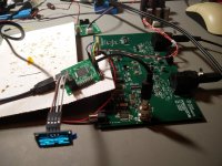
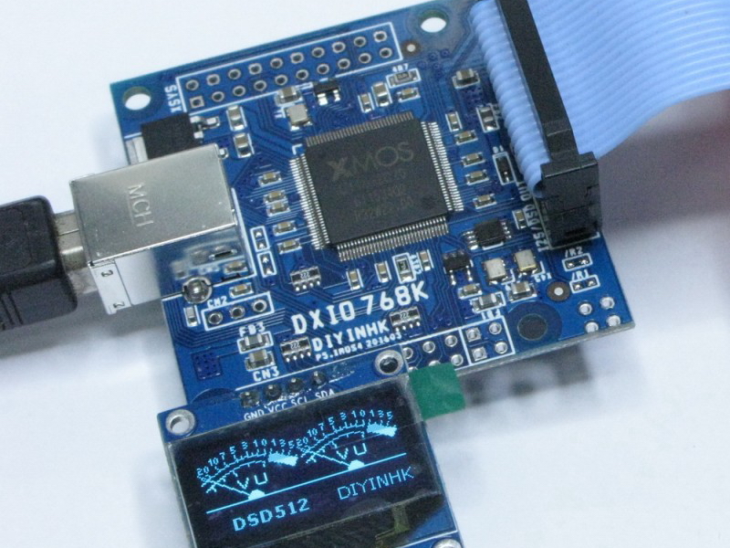
I've had this board for a few days now and it looks like it delivers. I've used it under Windows 10 to output stereo sound to a DAC as well as input sound from an ADC (PCM4222 EVM).
I made a little video of the board in action, connected to the OLED display.
https://www.youtube.com/watch?v=rwg9Qhb8AIg
Keep in mind that under Windows 10 it will only work in stereo (with DIYINHK's XMOS driver (v3.20)).
Also, if you want to use it with an ADC, you will need to slave the ADC to the XMOS.
Attachments
DimDim thanks for your help so far in order to get the board working!
Anyone here started coding for this xmos ? I have already connected to it with an xmos xtag-2, and trying to start a project. Not sure if there are any xmos programmers around here. Myself I have limited experience with XS1-L1.
diyinhk, a bit of help would be appreciated, a .XN file or a project skeleton based on the actual board implementation, would be very helpful. Having community-supported firmware enabling various other features, would surely help the sales of this wonderful minimalistic and powerful board!
DimDim thanks for your help so far in order to get the board working!
Anyone here started coding for this xmos ? I have already connected to it with an xmos xtag-2, and trying to start a project. Not sure if there are any xmos programmers around here. Myself I have limited experience with XS1-L1.
diyinhk, a bit of help would be appreciated, a .XN file or a project skeleton based on the actual board implementation, would be very helpful. Having community-supported firmware enabling various other features, would surely help the sales of this wonderful minimalistic and powerful board!
I have the XTAG3 and must get this board today or tomorrow and plan also to customize the Firmware for the AK4490 to get PCM 768khz and DSD256 following XMOS upgrade document for DSD 256 Native, i hope DimDim will provide me the source code of the XS1-L1 one, but i have already asked for the bin files two times without positve feedback yet, so without this help i will modify the USB Audio 2.0 source code from XMOS to cover the function to manage the DAC and Oscillator. Anyway help is welcome and learning by doing is the best way
")
Nice Work !
Dear tuxx,
Nice work ! Thank you for the inspiration !
All the best
Approx. two months ago I finally managed to finish the first part of this project:
The internals of the DAC:
An externally hosted image should be here but it was not working when we last tested it.
In general I am very much satisfied, although I am really interested in any suggestion of an additional iv stage that could be a part of this assembly.
Dear tuxx,
Nice work ! Thank you for the inspiration !
All the best
New USB to I2S 768Khz - DSD512/1024* Converter
Are you kidding? World's first 768k usb to i2s convertor from Hong Kong?
It's based on xmos, so it's from UK
Why do I need this 768k PCB? I do not have 768K music file to playback!
There are many technical advantage with this 768k PCB even when playback lower sampling rate music file:
1)The latest xmos xCORE-200 includes unique hardware divider and it is used to generate bit-clock from master clock directly.
2) The Xmos used in this pcb is XU216 2000MIPS and it contains two tile. It is equal to two XU208 combined in one chip, one dedicated tile is used for the USB data and the other tile is dedicated to process the audio data to the DAC.
3) This PCB uses linear regulator and it do not have onchip/onboard DC-DC switching converter. Thus it is power hungry:- 800mA maximum, 400mA typical (due to the use of all linear regulator) but it should also favour many people who do not like to use DC-DC convertor.
4) The xmos in this PCB is clocked directly from 45.158Mhz and 49.152Mhz audio oscillator, the timing and jitter can be better than those PCB uses 22.5792MHz 24.576Mhz audio oscillator as much as two time theoretically.
How do I test it is real 768K PCM is playing? I do not have 768k file!
User can download our computer generated precision pure 768Khz PCM test tone file to test(it is not recording from analog and thus zero background noise is achieved).
http://www.diyinhk.com/support/L1kR2kPCM768k24bit.rar
If the player/foobar setting is correct, user can measure LRCK=768kHz with an oscilloscope and DAC Left channel=1Khz, Right channel=2Khz sine wave output
AK4490 and AK4495 in hardware parallel control mode can playback 768K PCM immediately.
*DSD512 support in native mode (for windows requires >=v3.34 driver version) and DSD1024 theoretically work in laboratory test condition.
Feature:
1) Latest XMOS XCORE-200 2000MIPS 2 Tiles 16 Cores upto 2000MIPS in dual issue mode
2) 4 layer PCB, Solid ground plane (a must for high speed digital circuit)
3) NDK NZ2520SD Ultra low phase noise oscillator
Last edited:
The hardware divider is a new secret weapon from XMOS new xcore200 XU216 chip. Although it do not have must information disclosed yet, but you can try to look in the code for the new xc function configure_clock_src_divide()
I use Lecroy oscilloscope with JTA option enabled and active probe to compare the input(from clock) and output(from xmos pin) jitter, it is about the same and unbelievable, miles ahead from it's competitor! or there is no competitor as of now
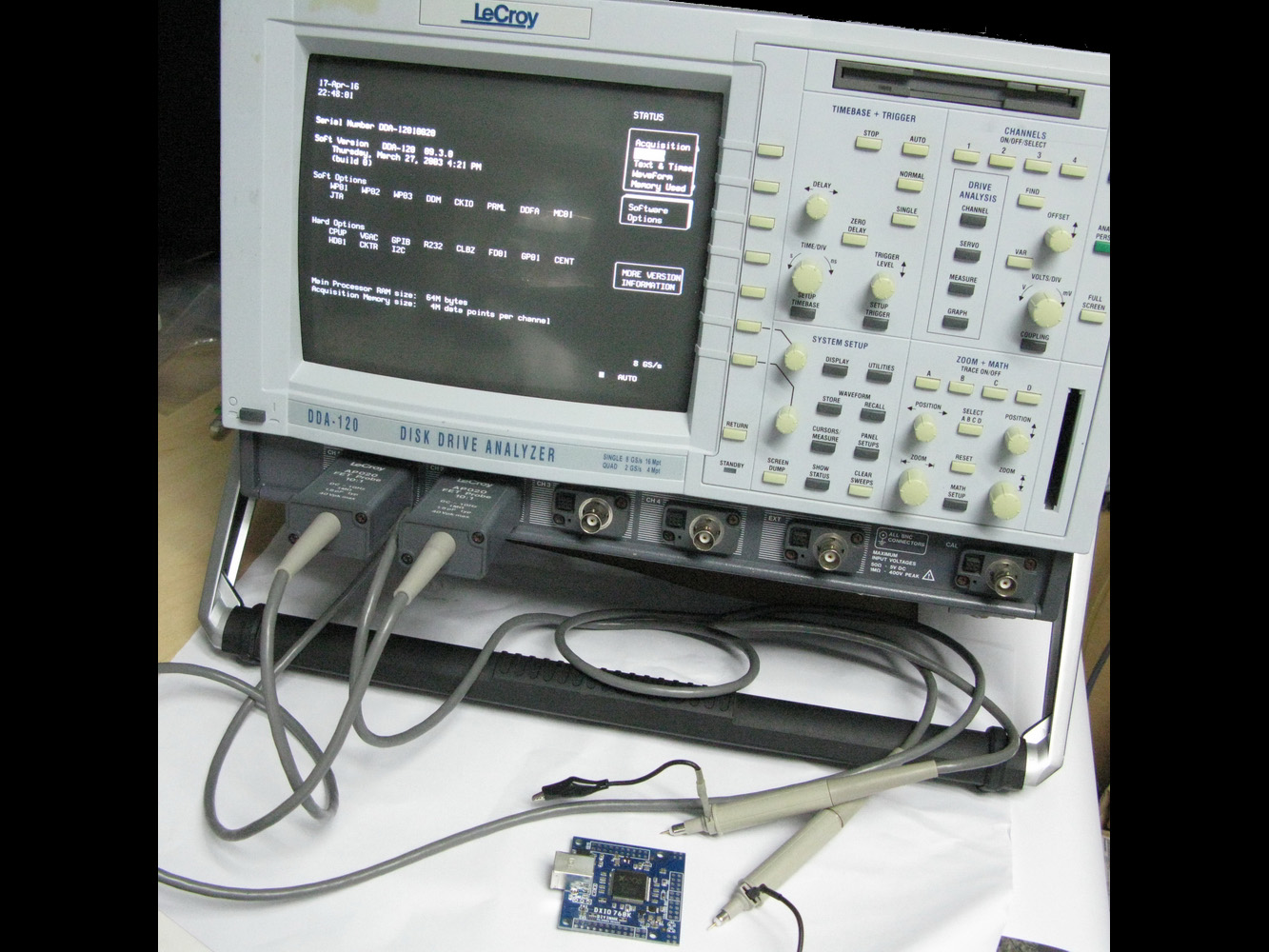
I use Lecroy oscilloscope with JTA option enabled and active probe to compare the input(from clock) and output(from xmos pin) jitter, it is about the same and unbelievable, miles ahead from it's competitor! or there is no competitor as of now
The hardware divider is a new secret weapon from XMOS new xcore200 XU216 chip. Although it do not have must information disclosed yet, but you can try to look in the code for the new xc function configure_clock_src_divide()
I use Lecroy oscilloscope with JTA option enabled and active probe to compare the input(from clock) and output(from xmos pin) jitter, it is about the same and unbelievable, miles ahead from it's competitor! or there is no competitor as of now
what is the competitor you are comparing with ? Also you can't really measure jitter with a cro because it has it's own sampling jitter and limited resolution. ie 1G/s CRO will have 1nS resolution.
Also what is the current consumption of this board ? Does it need its own power supply or can it run from from USB power ?
cheers
I am comparing the jitter between the input and output, not measuring the absolute value. It is the different
Measuring the absolute value requires a very precision setup, controlled environment and a monthly calibrate machine...This is not a general CRO, google Lecroy jitter dda has many information about it.
I do not have competitor, my competitor is always myself. I mean the xmos competitor, if it's exist
The max current consumption is about the same as the xmos xu216 official datasheet. It is powered from external regulated 3.3V. It is mostly following the reference design but with better onboard audio oscillator. If you want to test the capability of the xmos new xcore200 chip rather than built the cutting edge DAC, the official reference design PCB should be the way to go.
So, galvanic isolation/consequent reclocking has to be done off-board. Is there an option for supplying an external master clock?
The PCB includes full size sys connector and the user can flash the PCB with their customized firmware to includes any features. the xmos website contains all the information about xmos programming.
The onboard ndk clock is already the best But if you want to test the very expensive NDK DuCULoN
, user can remove the onboard oscillator and connect the external oscillator output and enable signal to the same soldering pad, please notes the solderpad is tiny and it can be tear out with the soldered wire.
Last edited:
- Home
- Vendor's Bazaar
- diyinhk Store