Hi, L.C.
Did-you made sure the improvement you noticed was not due to the add of the lytics to the main power Rail ?
By example strapping D+R, as you did, cutting the VAS+Input track, and use a regulated/cap multiplier to power them separately ?
This really question-me.
Hi Esperado

No, I am quite positive the improvement came from low Z connection between VAS and output stage. Also CCS's input bias current coming from the same rail potential as VAS resulting in much more SQ details. The only logical explanation would be ripple cancellation between both rails or unrippled modulation between input stage and VAS. CCS is connected to positve rails ripple and VAS to negative, so the influence of the ripple is canceled refering to GND potential, making less job for the feedback error correction, resulting in much more detail and transparency. Sort of speaking.
")
Thanks a lot for your response, Andrej.The only logical explanation would be ripple cancellation between both rails or unrippled modulation between input stage and VAS. CCS is connected to positve rails ripple and VAS to negative, so the influence of the ripple is canceled refering to GND potential, making less job for the feedback error correction, resulting in much more detail and transparency.
This means that, by luck, the ripple attenuation provided by the CCS is the same order than the VAS Gain ?
On my opinion, the only way to be sure that this improvement in listening experience is correlated with ripple is some verification like the one i suggested, because ripple suppression will be anyway a lot better with some cap multiplier
(remember my sims on this point: ). Both on common and differential.
I believe it is better to address the issue at the source. But i often noticed big changes with paralleled caps at the power rails, reason of my question.
This really intrigues-me, as it is an important aspect to ensure, in order to shoot right in the target in future CFA developments.
About low Z, it is referenced to ground, and, if cap multiplier provide 20db of extra rejection, this means that the impedance is reduced by a 10 factor, compared to D+R..
I'm a little maniac, each time i discover something that works, to understand why ;-)
Last edited:
Hi Christophe, that i agree if one shall learn. I like to follow when Esperado/Lazy Cat/sonnya go deep in circuit analyzing and hang on in head as good as i can (maybe 5-20% understanding.....I'm a little maniac, each time i discover something that works, to understand why ;-)
 ), would you accept my input which i think not been mentionen and it is the voltage to VAS goes up + and -0,9V, in other amps it is normal to have higher voltage than output devices. Else i can say the i am on Tea-Bag GB for Salas shunt REG delivered probably later in month, this have remote sense and ~0,001R(FET)/~0,007R(BJT) output Z in audio range and can just put out 45V. Where i wanna go is that if you/Andrej like listening test with such a PSU for Input/VAS i can do it if interest. The purpose for these PSU's was not VSSA, but my DAC and soundcard. I am just to go soldering VSSA in coming days and will make a little 1x2cm PCB on each side of VSSA module, then move R19/R20/D5/D6 to these PCB's inclusiv jumpers. This should give possibility for listening test with and without suggested shortening. In my SIM with Andrej's GB VSSA circuit the Fourier Analysis goes down from 0,0022204% to 0,0022166% harmonic distortion with shortening of R19/R20/D5/D6 (SIM: input 1,7V, Rails +/-45V, 78,56W into 8R, TR1/TR2/TR3 calibrated as in installation manual).
Last edited:
Means no changeIn my SIM with Andrej's GB VSSA circuit the Fourier Analysis goes down from 0,0022204% to 0,0022166% harmonic distortion .
.This microscopic difference is due to the higher VAS rail voltage without the filtering diodes (Diodes voltage drop).
About VAS, indeed, we can produce some more watts under 8 ohms if we provide ~ +-5 more volts to it than to the FET power devices. The purpose of L.C. in the VSSA design was obviously simplicity and quality more than max output power. (Not a big difference in acoustical level, anyway.).
And it is not a bad practice to limit the max signal excursion in VAS rather than by power device saturation.
About high quality low noise shunt regulators, they bring a real improvement at DACs reference pins. Or Low signal preamplifiers, regarding noise. We don't need such a precision/low noise in a power amp.
Thanks for your kind words.
Last edited:
Hi LC,
Did you start selling those enclosure yet? The one that supernet is selling looks really close to the one you were showing.
Ciao!
Do
My enclosure it is the same...6 of them were made as prototype, but they are all gone for now. If you want that case, then I recommend to you to buy allready made amplifier. Enclosure and heatsinks were quite expensive...and there are post cost too
If someone is interested into VSSA build with premium parts, I have one for sale:
Premium VSSA amplifier for sale
Premium VSSA amplifier for sale
LC I haven't yet received the amps, can you confirm that you have shipped and when?
Hi Odysseas
Last 30 VSSA PCB sets are waiting to be send out as soon as I'll get assembled PCB's from manufacturer.
I aligned numbers of received ALF mosfets and PCB's since there were inquiries up to the last piece. Cannot help for the time schedule since it doesn't depends just from me.
Remaining 7 GB members to receive VSSA as soon as possible:
milandks 4 PCB set
audionootje 4 PCB set
ua3grn 6 PCB set
Odysseas 4 PCB set
edbk 4 PCB set
woofertester 4 PCB set
Metallicus69 4 PCB set
Regards L.C.

Last edited:
With a BC560C/BC550C, 10K and 4.7µF ceramic, replacing original 10 Ohms, i got extra 22db of common mod ripple rejection (150mv 120Hz). A lot more at HF.
Nice test, bimo.
Without D+R, common mode noise climb from 50µV to 1mV (for 150mv) !!!
Differential from 3µV to 63µV....
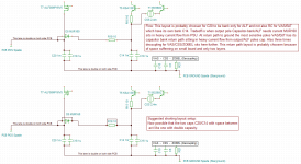
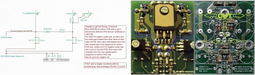
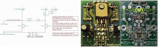
Evening post. I decoded the PCB lane routing for PSU as a schematic shown in picture 1 (See the text explanation in Picture). In picture 2 if this flow change routing for PSU lanes is done in my tubeguitar preamp, it is very very audioable. Picture 2 is best layout which i have learnt from books and experience. Picture 3 is easyer workaround way with little compromis in return path. Would it be audioable here and maybe cancel the R19/R20/D5/D6 shortening and keep concern for good PSU PSRR/CMRR in VAS/BJT input at good. Last if ALF pole is happier soundwise with the added capasitence, then exchange C20 with 1,5-2,2mF"......The reason of improvement (I believe you can lie on L.C. ears) is elsewhere, i think more and more the added caps at main power rails.
Attachments
Last edited:
I now realyze that previous post only holds schematic if screws/washers for the two VAS devices are isolated from PCB. Else two new chasis ground think with higher Z get into circuit. Think i will isolate here for controlling ground connections path. For clearness screw/washer at PCB for ALF is floating on board, so don't need isolation.Evening post....
Last edited:
TR1, TR2 - 5 k
TR3 - 1 k
From 260 sets already sent out there were app. 2-3 cases with trimming problems.
I had changed the trimmers and the situation is the same. I have this strange measurements of 56mV on TP3-TP4 and 1.60-2.60V (yep, volts) on TP1-TP2 swinging like it's listening to Benny Goodman. It does not sound distorted or anything, the sound level is close to the good working channel. I'm just still worried about this - it had problems with calibrating from the very beggining...
Nice one, BYRTT. Very clever analyze. Need at least to be tested by L.C to ensure if it is worth the dirt . (Ground tracks are so short).
Beware it can bring some evils with parasitic capacitances too...
... Or just by charging the ground tracks with a mono big enough coper wire soldered on it ? Not easy neither with SMDs across them.
This ground reference issue can explain the change noticed in the medium ? May-be. To be experienced.
To be remembered for future designs, anyway, an amp buster need a star grounding
Ps, i'm sure no need to any change +- power side if you keep diode+R on board. The 10 ohms makes enough difference, the distance is short and the external wires are still there, anyway...
. (Ground tracks are so short). Beware it can bring some evils with parasitic capacitances too...
... Or just by charging the ground tracks with a mono big enough coper wire soldered on it ? Not easy neither with SMDs across them.
This ground reference issue can explain the change noticed in the medium ? May-be. To be experienced.
To be remembered for future designs, anyway, an amp buster need a star grounding
Ps, i'm sure no need to any change +- power side if you keep diode+R on board. The 10 ohms makes enough difference, the distance is short and the external wires are still there, anyway...
It is R15=10R you measure over at TP1/TP2, and R16=10R at TP3/TP4. What is measured voltage TP1/TP2-TP3/TP4 at the good working channel this should be same here. Also compare with DMM the resistanse between TP1/TP2 and TP3/TP4 and same for good working channel, urgent that no power to amp is turned on in this measure. If lucky you just have bad R15, this R15 your solder iron had sit on for soldering emitter leg at T15, inspect both ends for R15.I had changed the trimmers and the situation is the same. I have this strange measurements of 56mV on TP3-TP4 and 1.60-2.60V (yep, volts) on TP1-TP2 swinging like it's listening to Benny Goodman. It does not sound distorted or anything, the sound level is close to the good working channel. I'm just still worried about this - it had problems with calibrating from the very beggining...
I remember LC was returning PCBs to get cleaned better, maybe small objects from this cleaning can be dried in area around your T5 device and makes this fluctuating. In very small area around T5 3x legs you have C8/C10 on top PCB, and R13/R15 bottom PCB, try cleaning this area with alcohol or acetone and check with glasses and measure with DMM that no leaking is present compared to good working channel (make R measures between 3 legs and compare to good channel).
Try weight my analize so you gets the less work to be done, could end to be worthless.
- Home
- Vendor's Bazaar
- VSSA Lateral MosFet Amplifier