Very nice circuit!
Yes indeed, usually we have double matched transistor at input, but here vice versa. Although we can put BC847BPN in input stage in no time.
")
Attachments
Khewwwwlll..... It's very easy for you, huh? Looking forward to see the highest (optimum) power possible with this topology (no less than 100W) without sacrificing the overall performance.
That would be CSA circuit, coming soon.
Hi LC,
need i some value tweakking to keep rail voltage to +/-35vdc as in first version (nice 625Va or 2x300va 2x25vac i have)
Marc
Rails can be +/-35-40V DC without any tweaking. This 1.1 version is just having a little more housekeeping, otherwise the same.
Rails can be +/-35-40V DC without any tweaking. This 1.1 version is just having a little more housekeeping, otherwise the same.
Thats cool....will spend a more little time on eagle.
Marc


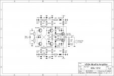
VSSA MosFet Amplifier V1.2
VSSA Amplifier schematic update. RCA input connector and speaker sign with impedance note added. This post is linked to from the first post of the thread to be easy accessible.
Again, this is very good simple amplifier, highly recommended.
Regards Lazy Cat
VSSA Amplifier schematic update. RCA input connector and speaker sign with impedance note added. This post is linked to from the first post of the thread to be easy accessible.
Again, this is very good simple amplifier, highly recommended.
Regards Lazy Cat
Attachments
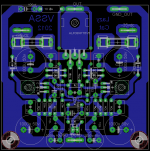
Here some tryout. BC847BPN is solder on bottom side. Board mesure 80x82mm
Very nice
An interesting option could also be to integrate power supply on this board. To have a simple plug & play amplifier.
Most logical way would be to have one rail on left side and other rail on the right side. That means...looking from left side to right side: dual rectifier diodes (TO220), two 4700/50V caps with SMD 0.15 ohm resistor at the bottom for CRC, main circuit, two 4700/50V caps, rectifier diodes. In short...similar like Fetzilla.
P.S.: Merry Xmas to you all too
Have you a link to this particular fetzilla aspect?
Marc
Have you a link to this particular fetzilla aspect?
Here and on the next page are some photos:
http://www.diyaudio.com/forums/aksa/191053-swordfishy-aspen-fetzilla-power-amp-100.html
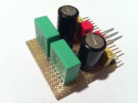
Preparing VSSA prototype for the action. PCB incorporates input BJT pair, trimmers and feedback capacitors. VAS and output ALF mosfet located on copper heatsink, small one but just enough for testing purposes
Attachments
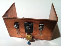
Preparing VSSA prototype for the action. PCB incorporates input BJT pair, trimmers and feedback capacitors. VAS and output ALF mosfet located on copper heatsink, small one but just enough for testing purposes
ADD gate resistors. Just for safety.
You Will have an lc oscillator due to the leadinductance together with the bypass capacitor from gate to gate .
My tests showed unstable bias due to oscillation. With even a small gateresistor it becomes stable.
Last edited:
Very nice
An interesting option could also be to integrate power supply on this board. To have a simple plug & play amplifier.
Most logical way would be to have one rail on left side and other rail on the right side. That means...looking from left side to right side: dual rectifier diodes (TO220), two 4700/50V caps with SMD 0.15 ohm resistor at the bottom for CRC, main circuit, two 4700/50V caps, rectifier diodes. In short...similar like Fetzilla.
P.S.: Merry Xmas to you all too
Thanks supernet
I have completely opposite idea to make VSSA as small as possible, to be versatile module for multi channel amp or an active speaker. I assume onboard PSU will be limiting factor here, you see, one big linear PSU or powerful SMPS can be used to supply all the channels at once, or dedicated linear PSU or SMPS for one channel only, in this way many combinations are possible regarding power supply.

Also this channel's PCB will be so small, one can use it for an output buffer of a signal generator or for the other testing purposes.

Double layered PCB with many SMD parts will be designed as soon as prototype will be extensively tested.

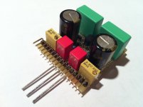
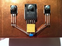
OK, thanks Sonny, there are two SMD resistors below 200R/MT bias trimmer, just not visible. As you can see 470R, 10R SMD resistors at 2SC/2SA transistors.
Ahhhh okay.
Dont you Think that it would be a good idear to replace the 15k with a bjt+jfet ccs to just make it more versatile.. >> same parameters across supply voltage range it Will be used In an active speaker.???
ADD gate resistors. Just for safety.
You Will have an lc oscillator due to the leadinductance together with the bypass capacitor from gate to gate .
My tests showed unstable bias due to oscillation. With even a small gateresistor it becomes stable.
I done my homework and read Application note for Alfets which I attached. On page 11 you can find a chapter Gate Resistor Recommendations where's formula to calculate Rg according to desired bandwidth and still to be on a safe side.
Attachments
Ahhhh okay.
Dont you Think that it would be a good idear to replace the 15k with a bjt+jfet ccs to just make it more versatile.. >> same parameters across supply voltage range it Will be used In an active speaker.???
First I'll test with resistor than will replace it with CSS. It intrigues me to inject current through resistor because it is theoretically in between two "constant" potentials, so in a way forced to source/sink constant current.
Also soundwise aspect interested me regarding comparison of both two options.
But you did change the ssa from resistors to ccs. What did the Sound image tell you???
SSA is completely different situation.
You have to read post #80 in this thread where I explained all three different possibilities to inject input bias current at this CFB topology. VSSA is different because current injection resistor is in between two AC grounds, so AC voltage drop on it is zero. DC voltage drop is high and almost constant so current is therefore constant as it would be CSS. See the idea ...
You have to read post #80 in this thread where I explained all three different possibilities to inject input bias current at this CFB topology. VSSA is different because current injection resistor is in between two AC grounds, so AC voltage drop on it is zero. DC voltage drop is high and almost constant so current is therefore constant as it would be CSS. See the idea ...
- Home
- Vendor's Bazaar
- VSSA Lateral MosFet Amplifier