PCB Layout Design Services - for prototypes OR serial products
I would like to announce that I design the PCB layout project in one layer, two layers or four layers. PCB projects can be used to manufacture PCB prototypes or large amounts of PCB's.
PCB layout projects can be presented in the following form: PDF files + Gerber 274X files, if you want to build PCB's in multiple copies to a specialized company + your prototype. Gerber format is 274X and is a format supported by many PCB manufacturers.
PCB projects are made keeping in mind the standard IPC2221 and another standard's.
1. The cost of developing a project will be (for circuits that operate in the frequency range 0 ... 20kHz):
Proiect Cost = 10...12 Euro / hour x number of hours available for development PCB project.
!!! Only in June 2019, all PCB layout design projects will elaborate with 8 Euro / hour.
2. For circuits that operate in the frequency range 20kHz ... 1GhHz cost will be:
2 layers PCB project:
Project Cost = 12...20 Euro / hour x number of hours available for development PCB project.
4 layers PCB project:
Project Cost = 20...30 Euro / hour x number of hours available for development PCB project.
Note the following: To develop a PCB layout project I will have to reproduce circuit diagram of the project in my software (informative, this process depends on the complexity of the schematic, it can take between 25 ... 60% of the time required to complete the PCB layout project, because we have built in some cases, new PCB footprint's).
ATTENTION!
i. In the case when PCB project would be carried out in a single layer (for example, in some cases when I can do the project in a single layer PCB), then the final price of the project will increase by 20...50%.
ii. My PCB projects using PCB net list. So, from this point of view PCB will follow as closely circuit diagram. This is a big advantage.
VERY IMPORTANT:
A.To tell you the exact price please send me your final version of the electronic schematic. The final version of the schematic is enough to have namely the wattage resistors and voltage capacitors, because I'll numbered electronic parts. Also, in the final schematic, please specify the integrated circuits package (DIP8, SOP14 ...), as well as their name because I need to know the numbering and name pins. So, is no need to tell me the values of the capacitors and resistors - not mandatory - that to protect your project, but the name must be specified for each integrated circuit and electronic component is SMD or THT (this must be specified for any electronic components directly on the diagram or schematic sent to me).
In this step I recommend you send me an excel file with what I said above.
B. Regarding the location of the connectors and what types of connectors you plan to use, you must send me a JPG image with the arrangement of these connectors and where you want to be placed holes for mounting PCB. In that picture it is necessary to present some significant share (distance holes from the margins PCB, mounting hole diameter - ie diameter 3.2 mm is typical - distances of the connectors to the PCB edges or margins…). At this stage you can send me and a PCB shape (or what is the desired format of the PCB board). I will analyze the format and tell you if it can fit in those dimensions circuit diagram. If don’t fit, then agreed with you, I'll take some decisions about the components used (ie if I use only THT or SMD components or both).
C. Performing design will cover three stages or phases:
For further details, additional information or questions, please post them in this topic or send me a private message: here, on diyaudio.com or my website Tehnium Azi. or new my e-mail:
donpetru - at - gmail dot com
I recommend you use my email address if you want to communicate quickly.
Payment will be made in advance through pay-pal after a preliminary discussion in which we establish conditions for project delivery and project execution time.
I assure the confidentiality of schematic submitted and that: I don't allow you to specify the values of passive components (like resistors and capacitors), plus it guarantees, that the confidentiality of the project.
!!!!!!!!!!!!!!!!!!!! If you want the project development in a professional setting you can find me on upwork.com com under user-name: PETRISOR D. But there the price for design will be higher. However, you do not have to worry because I am an honest person (known in many technical forums), but it's your choice, so you can call both ways: through this forum or using the website elance.com. I will give all my experience practice for PCB layout project results to be very useful and will bring money to you.
UPDATE: 19 february 2014:
If you want to develop projects of commercial audio amplifiers, I can provide support for:
- schematic amplifier design;
- improving the technical performance of the amplifier;
- construction and prototype testing and much more.
All these things can be negotiated with prices between: 10 and 25 Euro / hour.
LAST UPDATE: 09 June 2019:
I update price in Euro for PCB layout design.
I would like to announce that I design the PCB layout project in one layer, two layers or four layers. PCB projects can be used to manufacture PCB prototypes or large amounts of PCB's.
PCB layout projects can be presented in the following form: PDF files + Gerber 274X files, if you want to build PCB's in multiple copies to a specialized company + your prototype. Gerber format is 274X and is a format supported by many PCB manufacturers.
PCB projects are made keeping in mind the standard IPC2221 and another standard's.
1. The cost of developing a project will be (for circuits that operate in the frequency range 0 ... 20kHz):
Proiect Cost = 10...12 Euro / hour x number of hours available for development PCB project.
!!! Only in June 2019, all PCB layout design projects will elaborate with 8 Euro / hour.
2. For circuits that operate in the frequency range 20kHz ... 1GhHz cost will be:
2 layers PCB project:
Project Cost = 12...20 Euro / hour x number of hours available for development PCB project.
4 layers PCB project:
Project Cost = 20...30 Euro / hour x number of hours available for development PCB project.
Note the following: To develop a PCB layout project I will have to reproduce circuit diagram of the project in my software (informative, this process depends on the complexity of the schematic, it can take between 25 ... 60% of the time required to complete the PCB layout project, because we have built in some cases, new PCB footprint's).
ATTENTION!
i. In the case when PCB project would be carried out in a single layer (for example, in some cases when I can do the project in a single layer PCB), then the final price of the project will increase by 20...50%.
ii. My PCB projects using PCB net list. So, from this point of view PCB will follow as closely circuit diagram. This is a big advantage.
VERY IMPORTANT:
A.To tell you the exact price please send me your final version of the electronic schematic. The final version of the schematic is enough to have namely the wattage resistors and voltage capacitors, because I'll numbered electronic parts. Also, in the final schematic, please specify the integrated circuits package (DIP8, SOP14 ...), as well as their name because I need to know the numbering and name pins. So, is no need to tell me the values of the capacitors and resistors - not mandatory - that to protect your project, but the name must be specified for each integrated circuit and electronic component is SMD or THT (this must be specified for any electronic components directly on the diagram or schematic sent to me).
In this step I recommend you send me an excel file with what I said above.
B. Regarding the location of the connectors and what types of connectors you plan to use, you must send me a JPG image with the arrangement of these connectors and where you want to be placed holes for mounting PCB. In that picture it is necessary to present some significant share (distance holes from the margins PCB, mounting hole diameter - ie diameter 3.2 mm is typical - distances of the connectors to the PCB edges or margins…). At this stage you can send me and a PCB shape (or what is the desired format of the PCB board). I will analyze the format and tell you if it can fit in those dimensions circuit diagram. If don’t fit, then agreed with you, I'll take some decisions about the components used (ie if I use only THT or SMD components or both).
C. Performing design will cover three stages or phases:
- In the first phase of the project, after you send me the final version (including what I said in paragraphs A and B above), I communicate your project cost and period of the design (or timing of development of the design). If you agree, then move on to second part below.
- In the second part of the project, as things evolve right (example: we agreed on the price of the project), after you send me the final version of the schematic, I'll reproduce that schematic. To do this, you must pay in advance 10…50% of the project cost. So, you have to make payment through Pay-Pal, 10…50% of the project cost to redesign schematic (paypal fees are paid by the customer) and start PCB layout design. After I reproducing circuit diagram, I'll send you the PDF version of it to analyze (with 3D PCB Preview). Then you can do some corrections or additions (improvements) before moving effective to PCB layout routing.
- In the third part of the project will begin the actual design of the PCB. The remaining project cost can be paid within 1, 2 or 3 installments (or rates). Pay an installment involves continuous design. In the third stage does not allow schematic changes - is permitted only small changes in PCB fotoprint of active electronic components (like transistors or integrated circuits, but not resistors or capacitors).
For further details, additional information or questions, please post them in this topic or send me a private message: here, on diyaudio.com or my website Tehnium Azi. or new my e-mail:
donpetru - at - gmail dot com
I recommend you use my email address if you want to communicate quickly.
Payment will be made in advance through pay-pal after a preliminary discussion in which we establish conditions for project delivery and project execution time.
I assure the confidentiality of schematic submitted and that: I don't allow you to specify the values of passive components (like resistors and capacitors), plus it guarantees, that the confidentiality of the project.
!!!!!!!!!!!!!!!!!!!! If you want the project development in a professional setting you can find me on upwork.com com under user-name: PETRISOR D. But there the price for design will be higher. However, you do not have to worry because I am an honest person (known in many technical forums), but it's your choice, so you can call both ways: through this forum or using the website elance.com. I will give all my experience practice for PCB layout project results to be very useful and will bring money to you.
UPDATE: 19 february 2014:
If you want to develop projects of commercial audio amplifiers, I can provide support for:
- schematic amplifier design;
- improving the technical performance of the amplifier;
- construction and prototype testing and much more.
All these things can be negotiated with prices between: 10 and 25 Euro / hour.
LAST UPDATE: 09 June 2019:
I update price in Euro for PCB layout design.
Attachments
Last edited:
The offer by the end of December 2013:
For projects submitted in PDF format, the cost of developing a project will be:
Proiect Cost = Number of components assembly x 1 USD.
For example, if you have one schematic with 100 electronic components and if you want PDF format project, then the cost of the project will be: 100 x 1 USD = $ 100.
Offer valid only in the audio domain.
Last edited:
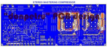
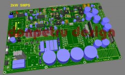
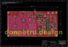
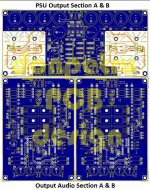
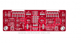
Other projects from my PCB portfolio (just a few).
All projects attached in this post are projects 100% made by me (development schematics, testing, PCB).
All projects attached in this post are projects 100% made by me (development schematics, testing, PCB).
Attachments
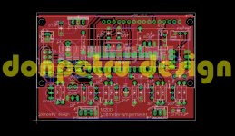
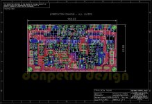
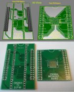
Another example of a PCB project in two and four pcb layers - from conception to reality.
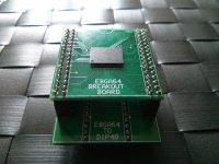
-------------- PCB quality and reliability --------------------
-------------- PCB quality and reliability --------------------
Attachments
Are you looking to manufacture PCB and printed circuits in United States? We have manufacturing services for printed circuit boards and PCBs for an installation available in USA.
Contact us to get comprehensive services for the design and manufacture of prototypes.
We are focused on providing high quality PCB design and printed circuit board assembly services at cost effective prices, as well as providing quick solutions according to the requirements of our customers.

Contact us to get comprehensive services for the design and manufacture of prototypes.
We are focused on providing high quality PCB design and printed circuit board assembly services at cost effective prices, as well as providing quick solutions according to the requirements of our customers.
- Status
- This old topic is closed. If you want to reopen this topic, contact a moderator using the "Report Post" button.
- Home
- Vendor's Bazaar
- PCB Design Services - for prototypes OR serial products