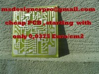
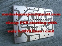
Hello everybody,
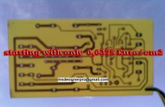
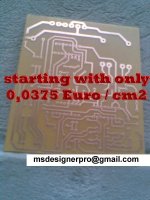
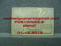
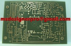
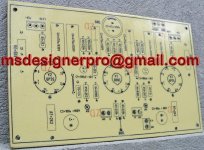
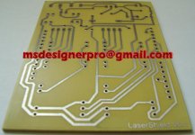
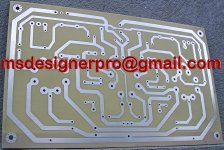
I present you attached the cheapest manufacturing way, for single pcb layer ( home made ) with semi-professional look , starting with 0,0375 Euro / cm2.
Can be also tinned, the copper traces ....or even something like " soldermask " ( can be solder through "soldermask" applied )
You can see also some more projects of mine to bellow address:
https://www.dropbox.com/sh/gz4t8fdnt0ylfu3/Fia1FUt9Yu
If someone ( without technical possibilities and required time ) need to build a prototype board or very small quantity ( up to 10 pcs / pcb ) , please feel free to contact me to : msdesignerpro@gmail.com
I can deliver you all over the world , in cheapest way , through National postal mail services.
Kind Regards,
MSdesigner Pro
E-mail: msdesignerpro@gmail.com
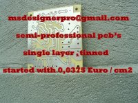
Attachments
Last edited:
Regarding file format for PCB's
Hi Benson,
I am from Romania.
If you export as pdf .....jpeg ....etc and you mention the sizes at corners is OK ! ....We can talk more details if yo'll send me email with required file to : msdesignerpro@gmail.com
See you there !")
Hi,
Where are you from?
Do you need gerber files? I'm working with a light version (TARGET3001) and cannot convert to gerber.
Greetz
Hi Benson,
I am from Romania.
If you export as pdf .....jpeg ....etc and you mention the sizes at corners is OK ! ....We can talk more details if yo'll send me email with required file to : msdesignerpro@gmail.com
See you there !
Hi Bensen,
I'm from Romania.
You can send me pdf , jpeg of file ....to : msdesignerpro@gmail.com
I suppose that you can export as jpeg otr pdf ...with at least 600 dpi ( resolution ) . Also menthion dimension at corners ( L x l )
Is not necessary Gerber file.
We can talk more by e-mail !
I look there !
I'm from Romania.
You can send me pdf , jpeg of file ....to : msdesignerpro@gmail.com
I suppose that you can export as jpeg otr pdf ...with at least 600 dpi ( resolution ) . Also menthion dimension at corners ( L x l )
Is not necessary Gerber file.
We can talk more by e-mail !
I look there !
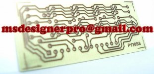
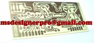
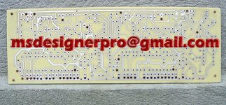
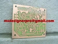
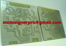
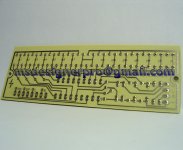
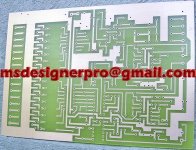
Some more printed circuit boards ( pcb's) , done it in last time can be seen it bellow:
Attachments
-
 CABLAJ-IMPRIMAT-PCB-1.jpg63.9 KB · Views: 621
 -
 CABLAJ-IMPRIMAT-PCB-2.jpg72.8 KB · Views: 642
 -
 Circuit imprimat pcb 20 - mic.JPG154.9 KB · Views: 687
 -
 CABLAJ-IMPRIMAT-PCB-3.jpg74.9 KB · Views: 730
 -
 CIRCUIT-IMPRIMAT-STANAT-PCB20.jpg123.2 KB · Views: 627
 -
 CABLAJ-IMPRIMAT-PCB-5.jpg196.5 KB · Views: 594
 -
 CIRCUIT-IMPRIMAT-STANAT-PCB-8.jpg230.5 KB · Views: 461
 -
 CIRCUIT-IMPRIMAT-STANAT-PCB-3.jpg176.5 KB · Views: 569
 -
 CIRCUIT-IMPRIMAT-STANAT-PCB-5.jpg574.8 KB · Views: 682
 -
 Circuit imprimat pcb 21.jpg238.4 KB · Views: 1,136
Thanks a lot for your appreciation.
I can't understand very well about " black pcb's".
What you mean ?
he means this material
160 x 100 mm 35µm Cu FR4 Platine schwarz kaufen - günstig bei OCTAMEX 160 x 100 mm 35µm Cu FR4 Platine schwarz bestellen - Datenblatt 160 x 100 mm 35µm Cu FR4 Platine schwarz
Thanks Birger.
Now is clear for me.
No I don't make it on black pcb.
Anyway , I have seen that this " black pcb " is for UV manufacturing procedure.
My procedure is an original one .....and is almost the same as " serigraphic procedure "
So is not as common way to manugature the pcb's , as UV ( photo ) or toner transfer.
Attachments
What is the purpose of a solder mask that can be soldered through.FR4 ( fiberglass ) pcb with transparent soldermask.
Can be solder through it.
I thought a solder mask was there to prevent soldering beyond the intended pad area.
Could you make some of these? Universal PSU, Capacitor and Diode Combination Board (Pre-scored and easy to snap into sections) - PCBs There's several forum members who are after them but they're not available from the store and little indication of when they will be available again...
Yes ! Andrew , in fact you have right soldermask is to prevent......but in fact is not a "real soldermask " .......it's something like a glossy flux ( dried ) which prevent oxides of copper traces and in the same time you can solder through pads ( help soldering ) ..............and of course you must be careful to solder only on the pad's places.
All the best.
All the best.
What is the purpose of a solder mask that can be soldered through.
I thought a solder mask was there to prevent soldering beyond the intended pad area.
Ordered five Fr4 tinned boards from Mihai and received them today.
They look really professional and I'm very happy with the result!
He finished them during weekend a couple of days after payment and shipping was really fast too!
I just wanted to write a good review here so you may feel confident about ordering from him. Communication via email was great, and it was a pleasure to deal with him.
I will not make through plate holes , because inquiry is under 1% !
The traces on FR4 ( better than CEM , XPC , if required many re-solderings) , are strong enough.
Re-soldering is helped if traces are tined from beginning.
Re-soldering " traces- pad's life" it depends of soldering skills ( soldering time , de-soldering time) , soldering temperature , de-soldering temperature.
If you want, we can talk more to : msdesignerpro@gmail.com
I can answer you much faster through above e-mail.
All the best,
Mihai
Do you have plated through holes?
How well do the traces survive removal of component lead and re-soldering?
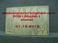
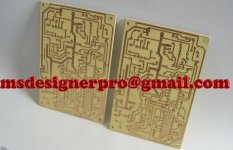
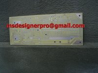
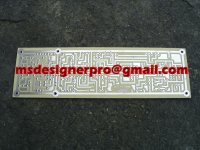
Hello everybody !
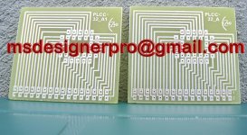
Bellow you can see the latest pcb's done it on FR4 and CEM support.
Two of them, are tin plated.
If anyone without technical possibilities is interested, I can help him in fastest way , and cheapest way , including delivery all over the world with National Post Mail Services.
All the best,
Mihai
Bellow you can see the latest pcb's done it on FR4 and CEM support.
Two of them, are tin plated.
If anyone without technical possibilities is interested, I can help him in fastest way , and cheapest way , including delivery all over the world with National Post Mail Services.
All the best,
Mihai
Attachments
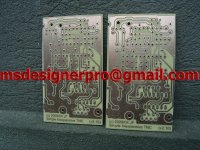
Hello everybody !
Bellow you can see my latest pcb's done it on FR4 and CEM support.
Two of them, are tin plated.
If anyone without technical possibilities is interested, I can help him in fastest way , and cheapest way , including delivery all over the world with National Post Mail Services.
All the best,
Mihai
Bellow you can see my latest pcb's done it on FR4 and CEM support.
Two of them, are tin plated.
If anyone without technical possibilities is interested, I can help him in fastest way , and cheapest way , including delivery all over the world with National Post Mail Services.
All the best,
Mihai
Attachments
Last edited:
- Home
- Vendor's Bazaar
- Cheap printed circuit boards starting with 0,0375 Euro / cm2