Hi !
If I understood correctly, you are interested for double side printed circuit board.Please send me your double layer board to msdesignerpro@gmail.com , and I'll see if I can help you.
Please note that the best quality ( about holes through layers) will be done if you can send me Eagle , ExpressPCB ........etc files. ( .brd.......etc )
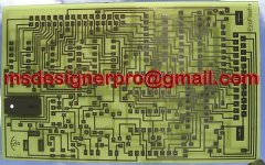
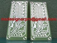
Attached is latest DOUBLE SIDE printed circuit board, just did it in this weekend.
All the best,
Mihai
If I understood correctly, you are interested for double side printed circuit board.Please send me your double layer board to msdesignerpro@gmail.com , and I'll see if I can help you.
Please note that the best quality ( about holes through layers) will be done if you can send me Eagle , ExpressPCB ........etc files. ( .brd.......etc )
Attached is latest DOUBLE SIDE printed circuit board, just did it in this weekend.
All the best,
Mihai
How about double sided boards? Are able & willing to make such?
Attachments
Last edited:
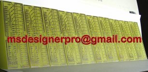
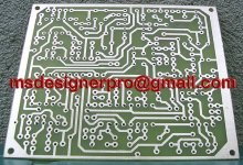
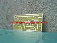
Below you can see 10 pcb's done it for one graphic equalizer for a friend of mine.
Any inquiry for tinned FR4 printed circuit board to : msdesignerpro@gmail.com
Any inquiry for tinned FR4 printed circuit board to : msdesignerpro@gmail.com
Attachments
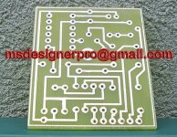
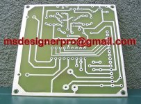
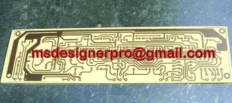
Below, you can find my newest 3 tinned pcb's released this weekend.
Any inquiry for tinned FR4 printed circuit board to : msdesignerpro@gmail.com
Any inquiry for tinned FR4 printed circuit board to : msdesignerpro@gmail.com
Attachments
Any inquiry for tinned FR4 printed circuit board to : msdesignerpro@gmail.com
Attachments
Any inquiry for tinned FR4 printed circuit board to : msdesignerpro@gmail.com
Attachments
")
Thanks lanchile, for your appreciation.
If you have something to be done I'll be happy to help you.
So,I look for your e-mail to : msdesignerpro@gmail.com
If you have something to be done I'll be happy to help you.
So,I look for your e-mail to : msdesignerpro@gmail.com
Could you be more clear ?
What you mean ?
What you mean ?
Has anyone used these ? I bought some cheap PCBs the other week, the first one blew up, the second one went into the bin. I hasten to add that they were not from this guy.
On FR4 fiiberglass the quality is OK ! ( look above feedback from Francisco Perez -Spain ) .........he was very happy for my release.
On CEM3 support ( yellow , nontransparent ) here we cal talk about diferent quality of boards ( some of them could not be strong enough if you solder /unsolder for too much times.
Anyway I don't use also this kind of CEM3.
But in general , even on FR4 could be the same if you use a not correctly temperature of solder station when you solder / unsolder.
TINNING is very helpful for soldering.
I consider that my pcb's are looks great for a home-made release.
If I can do it them in cheapest way don't means that have low quality.
All the best,
Mihai
You pay your money and you takes your choice.
I bought some cheap PCBs and they were utter rubbish.
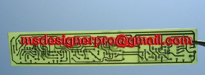
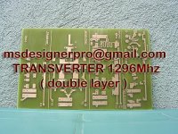
Bellow can be found , the just released printed circuit board , double layer , on fiberglass support.
The backside layer is "untouched" because is the screen of transverter 1296 Mhz.
The quality of pcb is amazing if we take in consideration that has been done from a very old scanned document with less than 200 dpi grey, resolution.
The backside layer is "untouched" because is the screen of transverter 1296 Mhz.
The quality of pcb is amazing if we take in consideration that has been done from a very old scanned document with less than 200 dpi grey, resolution.
Attachments
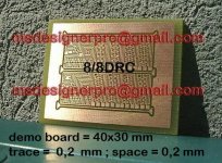
KatieandDad, I already uploaded above a DEMO BOARD
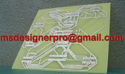
Below you can see my DEMO BOARD = traces = 0,2 mm , spaces=0,2 mm
Below you can see my DEMO BOARD = traces = 0,2 mm , spaces=0,2 mm
Can you please detail the minimum track width and minimum track clearance that your process can accurately deal with.
- Home
- Vendor's Bazaar
- Cheap printed circuit boards starting with 0,0375 Euro / cm2