hayenc said:Are you looking to do the AGND to VGND connection like on the eval board? It is a zero ohm resistor under the chip on the reverse side of the board.
Yeah, AGND to DGND. The only way to insure they have the same potential is to join them. I see now how the eval board did it, I wonder if that is the best/good enough, or if there is a better way...
hayenc said:Russ,
Do you expect any problems with the variable input impedance of the JT on Opus?
Not unless it drops below the minimum load for the DAC. I would expect it to be fine. One can also alter the JT so that it has a constant input impedance, but thats for another thread.
")
BrianDonegan said:I was actually thinking of using a balanced TS stage immeadiately after the DAC as a sort of buffer/line driver, probably at unity gain, in the same case, then going off to JT and TS or X-BoSoZ in my preamp.
You could do that, but I doubt the buffer stage would be necessary.
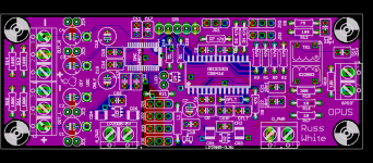
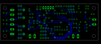
Russ White said:What I did was joined the two planes at a single spot with a very thin trace.. That way people can simply cut the trace if they like, or connect a ferrite or something between an AGND pad and a DGND pad.
That very probably is a good solution and won't need a change at all. The PCB looks OK and complete, certainly for a beta version. I do not see errors although I do not have enough time to reread datasheets of both the chips so I might not see mistakes. I hope rfbrw is around to check things over. Series and/or termination resistors for I2S use would have been nice but the board would have to change too much.
A power PCB with separated supplies of a 2 x 6V 250 to 500 mA transformer, Schottky diodes and caps + extra filtering ( common mode coils ) and the same dimensions as the DAC board would be handy for testing. Or am I asking too much now ?
Those small regs will be a challenge for my hands and eyes...
Hi Russ,
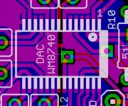
This ground link under the chip might or might not be a good idea...
http://www.tentlabs.com/page19/page24/page35/files/Supply_decoupling.pdf
Very interesting file.
This ground link under the chip might or might not be a good idea...
http://www.tentlabs.com/page19/page24/page35/files/Supply_decoupling.pdf
Very interesting file.
I suppose you mean this part...
I have seen both sides of this argument more times than I can count, yet I do admit to being new enough at this science (and art) to not be authoritative on the subject. That said, in the end practicality must prevail. I do have to "actually" finish this thing you know. My solution is close to the manufacturers own, so it must be close to acceptable. I hope..
Layers
With nowadays clock-speeds at least a double layer board must be used in order to meet
European emission limits and to maintain signal integrity. We can assign one layer as a
groundplane. This layer will be the closest to the ICs (component side) and act as an electrical
screen as well. For high frequencies (practice shows > 200 MHz) the die of the IC starts acting
as an electrical mono-pole. Reduction of this type of emission has been shown useful by Jon
Marks’ article.
With the described decoupling philosophy signals interacting between ICs will always run
through the groundplane, regardless of the transaction (high to low or low to high). As the
supply lines do no longer carry RF currents (at least, if you have followed the instructions in
the first half of this article).
This enables us to create neat transmission lines between ground-plane and signal trace. Due
to the use of series resistors and inductances, lots of bridges appear, effectively reducing the
number of via’s usually necessary.
Supply lines can be routed as a last step. Inductances have been added so the RF current
through these lines is heavily reduced; their routing has become non-critical, as they only carry
dc currents.
Never use power planes. It is not needed, as dc-supply currents only need small traces. A
power plane may resonate with the groundplane: your PCB will act as dipole antenna!
Keep the groundplane closed
One final word to finish. Very often the groundplane is intersected by a slot, between the
analogue and digital part of the PCB. The two planes are then connected beneath the AD or
DA converter chip, or even worse at the supply-lines entry on the PCB (as advised by some IC
manufacturers). With the planes separated, signal currents that cross the intersection are
forced to return via the groundplane and as such need to describe a huge loop, around the
intersection. This leads to high emission, and higher chance on inter-system pollution.
Recently a friend followed the measures described in this article, on a commercially available
AD-converter (a demo board from a well-known manufacturer). Improvements finally
decreased emission with 30 dB and enhanced both jitter and audio performance.
By taking appropriate measures, we know the whereabouts of amplitude, frequency-content
and domain of the currents on the PCB. By shorting currents on a local basis, the currents
through the plane are known as well the area they run in. We now can keep the plane closed
and profit from all the advantages.
I have seen both sides of this argument more times than I can count, yet I do admit to being new enough at this science (and art) to not be authoritative on the subject. That said, in the end practicality must prevail. I do have to "actually" finish this thing you know.
My solution is close to the manufacturers own, so it must be close to acceptable. I hope.. Russ White said:
I have seen both sides of this argument more times than I can count, yet I do admit to being new enough at this science (and art) to not be authoritative on the subject. That said, in the end practicality must prevail. I do have to "actually" finish this thing you know.
That counts for me too. But I know Guidos expertise in this matter and trust his opinion. Maybe the trace can be 7 times wider so that the planes really are connected ? It still can be cut with a Dremel if one wishes to connect groundplanes with a ferrite bead or 0 Ohm resistor.
Guido's comments about power planes seem to agree with much of what I have read from other sources, as normally power planes are used as internal layers in four or more layer boards that have ground planes as the outside layers on both sides.
However, if you follow all our suggestions you will probably end up with a completely different board to the one you posted to start with, and a redesign that will take months!
However, if you follow all our suggestions you will probably end up with a completely different board to the one you posted to start with, and a redesign that will take months!
Nixie said:What's the worry with emissions if the DAC is in a metal enclosure?
One final word to finish. Very often the groundplane is intersected by a slot, between the
analogue and digital part of the PCB. The two planes are then connected beneath the AD or
DA converter chip, or even worse at the supply-lines entry on the PCB (as advised by some IC
manufacturers). With the planes separated, signal currents that cross the intersection are
forced to return via the groundplane and as such need to describe a huge loop, around the
intersection. This leads to high emission, and higher chance on inter-system pollution.
Recently a friend followed the measures described in this article, on a commercially available
AD-converter (a demo board from a well-known manufacturer). Improvements finally
decreased emission with 30 dB and enhanced both jitter and audio performance
We dislike jitter and we like audio performance don't we ? Also plastic enclosures are cheaper than metal ones

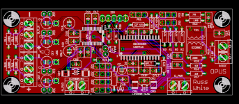
Are you sure this is still a beta version Russ ? It is looking better by the day. To be honest I did not even see the powerplane, probably because the colors resemble eachother on the picture.
No serious link really. In Guidos papers he gives an example of lowering emission by 30 dB by doing the groundplane "the right way". He states that less EMI emission means better specs, less jitter and better sound.
Nixie asked why bother about EMI when the DAC is being built in a metal box. Well, less emission internally despite using a metal box also means better specs, less jitter and better sound...
BrianDonegan said:What's the link between enclosure and emissions there?
No serious link really. In Guidos papers he gives an example of lowering emission by 30 dB by doing the groundplane "the right way". He states that less EMI emission means better specs, less jitter and better sound.
Nixie asked why bother about EMI when the DAC is being built in a metal box. Well, less emission internally despite using a metal box also means better specs, less jitter and better sound...
- Status
- This old topic is closed. If you want to reopen this topic, contact a moderator using the "Report Post" button.
- Home
- More Vendors...
- Twisted Pear
- Mr White's "Opus", designing a simple balanced DAC