The output are going through caps so that the DAC output can be used directly. They are AC coupling caps. If you did not have them the outputs would be at DC potential. If you intend to have coupling caps at some other place(say a filter circuit) you could simply jumper the caps on this PCB. In short the caps are there to block the DC. Pretty much standard on a DAC output.
Hi Russ ")
I missed this thread!
Glad to see your interests are growing
Maybe a high quality active crossover is in your future
When you get tired of your Wolsom DAC, PLEASE consider the following chips form AKM:
*sample rate converter AK4122 and AK 4124.
*DAC chips AK4193, AK 4195 and AK 4196 (the later is new, I don't know if it fits)
I would make an upsampler DAC (all I2S Ins/Outs) myself IF i had the knowledge and could source them. To my ears, there is definitelly an improvement in resolution and lower sound floor when upsampling
(yet I use a NOS DAC also )
Best of lucks!
M
I missed this thread!
Glad to see your interests are growing
Maybe a high quality active crossover is in your future
When you get tired of your Wolsom DAC, PLEASE consider the following chips form AKM:
*sample rate converter AK4122 and AK 4124.
*DAC chips AK4193, AK 4195 and AK 4196 (the later is new, I don't know if it fits)
I would make an upsampler DAC (all I2S Ins/Outs) myself IF i had the knowledge and could source them. To my ears, there is definitelly an improvement in resolution and lower sound floor when upsampling
(yet I use a NOS DAC also
)Best of lucks!
M
Have you thought about adding in a PCM2902 with all surface mount stuff for a USB input? There is a bit of extra space on the board and you might be able to just add it to this board instead of having another board for just the USB. People can just leave off all the parts if they are not looking for that feature. I think it would be about 16 more parts including the USB header. Oh, if I'm babbling or this is contrary to the design goals just ignore me.
-Naz
-Naz
Hi guys,
Thanks for the input, I will consider adding USB. if it will fit the PCB as I have it sized. Optical input can actually be done with the current PCB, its just some of the components would be off the PCB.
I would really appreciate some input about my schematic. Is the reset scheme OK? I have heard nothing really on that. Does the basic schematic look OK? I want to get some protype PCBs made, but I don't want to waste money on a circuit that has no chance.
Remember this is my first DAC design. I really need lots of eyes looking at this and giving me plenty of hints.
Thanks!
Cheers!
Russ
From what I am reading (though I could be wrong) the reset only really needs to occur at power up. So I used a TPS3809 which should do the trick. I also went ahead and had it reset the DAC too, but the DAC datasheet does not say this required. I just thought it would be safe.
Cheers!
Russ
Here is the current schematic...
Cheers!
Russ
Here is the current schematic...
Attachments
Russ
555 from this site?
http://sound.westhost.com/project85.htm
could be triggered when changing sourses ie usb spdif etc
allan
555 from this site?
http://sound.westhost.com/project85.htm
could be triggered when changing sourses ie usb spdif etc
allan
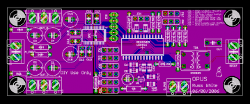
And here is the layout so far. I think I will stick with the USB input as second PCB because I want to isolate it more completely with its own power supply and such.
The transformer provided complete isolation of the SPDIF signal, so I see no particular advantage to putting optical input dircetly on the PCB. You can still use it, just panel mount the components and run the input to the DAC side of SPDIF input trafo.
I am really trying to follow the K.I.S.S principle on this first go.
Allan, I had looked at the 555 soluton before, but I don't think it fully applies to the CS8416, as according the spec sheet the CS8416 sort of soft resets when it loses and regains the incoming clock, same for the DAC.
Here is the layout right now:
Cheers!
Russ
Attachments
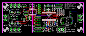
Russ, this might sound like an odd request, but my color blindness (red-deficent) is making it hard to see all the traces on your board. I don't know what program your using, but if there is an easy way to change the color scheme, I'd appreciate a "color-blind friendly" version (blues, blacks, greens). If not, I'll just squint really, really hard at it. If this qualified for "strange post of the day", I apologize in advance.
Russ White said:And here is the layout so far. I think I will stick with the USB input as second PCB because I want to isolate it more completely with its own power supply and such.
The transformer provided complete isolation of the SPDIF signal, so I see no particular advantage to putting optical input dircetly on the PCB. You can still use it, just panel mount the components and run the input to the DAC side of SPDIF input trafo.
I am really trying to follow the K.I.S.S principle on this first go.
Allan, I had looked at the 555 soluton before, but I don't think it fully applies to the CS8416, as according the spec sheet the CS8416 sort of soft resets when it loses and regains the incoming clock, same for the DAC.
Here is the layout right now:
Cheers!
Russ
all it needs is reset at power up.
switching between sources it will reset itself?
then simplist is the best.
allan
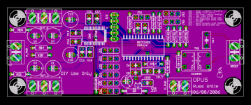
Russ, a point or two if I may.
There is no isolation between the CS8416 output and the I2S connector. It is therefore possible for the two outputs to drive each other. Not good. You might want to consider a TTL switch.
The deemphasis bits in the WM8740 should be set by the CS8416 which in turn will be triggered by the deemphasis flag in the SPDIF datastream. I find it unlikely that anyone will open a up case to set the deemphasis bits. I know I wouldn't, I only have one CD that triggers the deemphasis flag.
Finally, you might want to provide the option of having the CS8416 or the external source trigger MUTEB when there is no data.
Someone please translate this:
It's from http://www.edn.com/article/CA426064.html and you can see the figure referred to in the text at http://www.edn.com/contents/images/426064f3.pdfWolfson's WM8740 embodies an interesting variation on the usual multibit delta-sigma DAC architecture. A DEM block with 14 nonequally weighted elements decomposes 6-bit PCM words in several cascaded stages. The 8740's DEM array includes two unity elements and two 2×, two 4×, and eight 8× elements. Individual elements combine in like or dissimilar polarity based on the LSB at each stage. After acting on the LSB, each stage passes on the remainder to the stage that follows. At the end of the cascade, the final remainder feeds a nonweighted DEM block. The 8740's DEM blocks use random-number sequences in the element-selection process to prevent the occurrence of tones on the output that repetitive element-access patterns can generate in the presence of small nonidealities in individual elements.
The result of Wolfson's unequally weighted DEM block is a substantial reduction of out-of-band noise compared with conventional DACs based on multibit delta-sigma modulators (Figure 3). The DAC's in-band SNR is 110 dB in 20 kHz at 48k samples/sec. THD is –95 dB or better.
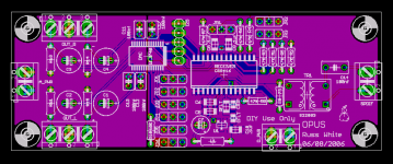
Opus ready to fly... I think...
OK folks,
Time for beta prototypes.
For you beta testers here is what I am going to get made (there still is a little time if you see anything wrong, but only a few hours...)
Keep in mind that I2S header is for playing around with external receivers and debugging and such. If you use you would omit the on board receiver. The PCB s not designed to use both at the same time. You could also use just the receiver and pipe I2S to another DAC if you omit the DAC.
I have several emails from interested beta testors. You will have an opportunity to order a beta board. We will only allow 10 beta testers. Beta testers will get a complete kit at our cost + shipping.
Here is an image of the PCB without the copper pours for clarity.
Cheers!
Russ
Attachments
- Status
- This old topic is closed. If you want to reopen this topic, contact a moderator using the "Report Post" button.
- Home
- More Vendors...
- Twisted Pear
- Mr White's "Opus", designing a simple balanced DAC