You'd be bandwith limited to about 600KHz...
So we could get to 30kHz with 20kohm output impedance?
Wich means,for a pretty novice,no good ,or...Teoretically, yes
Trying do make up my mind wich way to go..
I would aim for an even lower source impedance, preferably not more than a couple of hundred ohms.
In my experience powerful driver stages always sounds better than whimpy ones, even if both technically are capable of driving the load. This goes for both tube and mosfet output stages.
Just my two cents")
In my experience powerful driver stages always sounds better than whimpy ones, even if both technically are capable of driving the load. This goes for both tube and mosfet output stages.
Just my two cents
My 2 cents worth also:
You need much greater bandwidth in the gate driver than you might think to avoid distortion. Here’s why:
The driving resistance, whether it’s the plate resistance of a common-cathode stage or the cathode resistance of a CF, and the gate capacitance form a roll-off together at a pole frequency of 1/(2*pi*R*C). At that pole frequency, amplitude drops by 3dB and phase is shifted by 45 degrees. At one tenth of the pole frequency (perhaps down into the “audio band”), amplitude drops by only 0.043 dB and phase shift is -5.7 degrees.
So if the pole is set to 200KHz, as a convenient example, then if we look at the top of the audio band at 20KHz, the amplitude is down by only 0.043dB and the phase is retarded (“delayed”) by 5.7 degrees. That equates to 0.8 microsecond of “delay” at 20KHz. That doesn’t sound too scary.
So what?
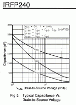
In the case of the IRFP240, we need to worry primarily with Crss (= Cdg) which in the follower configuration is not amplified by the Miller effect happily. But it’s bad enough. (We’ll ignore the bootstrapped Cgs for simplicity). At the operating point of around 11 volts drain-to-source (Vds), Crss is about 350pF. To achieve a 200KHz roll-off (just for sake of example) we’d need to drive it with a resistance of no higher than about 2200 ohms, which is easily achievable with a decent triode’s plate. Is all well then? No, read on...
Vds can vary by almost +/- 10 volts from this operating point as it swings with signal. The problem is that Crss varies from about 200pF at Vds = 20 volts to about 1300pF at Vds = 1. This means that the RC time “constant” that determines the pole frequency and phase shift is not constant at all; it varies dramatically with signal voltages. This variation creates a phase intermodulation mechanism that defines, I believe, the difference between the sounds of MOSFETs and tubes. I believe that some people equate phase intermodulation with detail and etching, when it fact it’s false detail and distortion.
Taking the simple math one step further for this example (bear with me): As I said, when the output signal approaches the peak positive level, Crss approaches 1300pF. Driven by our hypothetical 2200 ohm driver, the pole frequency then drops from 200KHz to about 54KHz. Looking again at the amplitude and phase shift effects at 20KHz we see an amplitude drop of 0.55dB and a phase shift of -20.3 degrees. So the gain at 20 KHz actually CHANGES as the signal swings, from -0.043 dB to -0.55dB. And phase shift grows from -5.7 degrees to -20.3 degrees at 20KHz. When several frequencies are introduced into the amp at the same time (i.e. music) these signals will intermodulate with each other in both time and amplitude.
Converting that phase shift to time at 20 KHz, the high end of the audio band is delayed by an additional 2 microseconds as the signal swings positive (and by a lesser amount in the other direction too, which we’ll ignore). That’s 2,000 nanoseconds or 2,000,000 picoseconds. You can think of this as a kind of jitter. In the digital world, we’ve learned that the ear is exquisitely sensitive to jitter. We believe that jitter down into the hundreds of picoseconds may still be audible. Granted, not all jitter mechanisms are alike. But what we have in this example is a peak “jitter” of about 2,000,000 picoseconds. Across a lesser signal swing or at lower audio frequencies we might see “only” 2,000 to 20,000 picoseconds of jitter. That range is still orders of magnitude more than we would hope for.
Design implication: The MOSFET’s gate needs to be driven from a very, very low drive resistance to force the pole to a very high frequency where lingering phase shift in the audio band is reduced. At the very least, the gate deserves a CF driver using a high mu, high gm tube, and even that may not be enough. IMO, of course.
Edit: These numbers seem worse than even I would have predicted. I hope that someone will check my math and make sure that I didn't make a mistake. The message is still valid though, even if a decimal point is off by a space.
You need much greater bandwidth in the gate driver than you might think to avoid distortion. Here’s why:
The driving resistance, whether it’s the plate resistance of a common-cathode stage or the cathode resistance of a CF, and the gate capacitance form a roll-off together at a pole frequency of 1/(2*pi*R*C). At that pole frequency, amplitude drops by 3dB and phase is shifted by 45 degrees. At one tenth of the pole frequency (perhaps down into the “audio band”), amplitude drops by only 0.043 dB and phase shift is -5.7 degrees.
So if the pole is set to 200KHz, as a convenient example, then if we look at the top of the audio band at 20KHz, the amplitude is down by only 0.043dB and the phase is retarded (“delayed”) by 5.7 degrees. That equates to 0.8 microsecond of “delay” at 20KHz. That doesn’t sound too scary.
So what?
In the case of the IRFP240, we need to worry primarily with Crss (= Cdg) which in the follower configuration is not amplified by the Miller effect happily. But it’s bad enough. (We’ll ignore the bootstrapped Cgs for simplicity). At the operating point of around 11 volts drain-to-source (Vds), Crss is about 350pF. To achieve a 200KHz roll-off (just for sake of example) we’d need to drive it with a resistance of no higher than about 2200 ohms, which is easily achievable with a decent triode’s plate. Is all well then? No, read on...
Vds can vary by almost +/- 10 volts from this operating point as it swings with signal. The problem is that Crss varies from about 200pF at Vds = 20 volts to about 1300pF at Vds = 1. This means that the RC time “constant” that determines the pole frequency and phase shift is not constant at all; it varies dramatically with signal voltages. This variation creates a phase intermodulation mechanism that defines, I believe, the difference between the sounds of MOSFETs and tubes. I believe that some people equate phase intermodulation with detail and etching, when it fact it’s false detail and distortion.
Taking the simple math one step further for this example (bear with me): As I said, when the output signal approaches the peak positive level, Crss approaches 1300pF. Driven by our hypothetical 2200 ohm driver, the pole frequency then drops from 200KHz to about 54KHz. Looking again at the amplitude and phase shift effects at 20KHz we see an amplitude drop of 0.55dB and a phase shift of -20.3 degrees. So the gain at 20 KHz actually CHANGES as the signal swings, from -0.043 dB to -0.55dB. And phase shift grows from -5.7 degrees to -20.3 degrees at 20KHz. When several frequencies are introduced into the amp at the same time (i.e. music) these signals will intermodulate with each other in both time and amplitude.
Converting that phase shift to time at 20 KHz, the high end of the audio band is delayed by an additional 2 microseconds as the signal swings positive (and by a lesser amount in the other direction too, which we’ll ignore). That’s 2,000 nanoseconds or 2,000,000 picoseconds. You can think of this as a kind of jitter. In the digital world, we’ve learned that the ear is exquisitely sensitive to jitter. We believe that jitter down into the hundreds of picoseconds may still be audible. Granted, not all jitter mechanisms are alike. But what we have in this example is a peak “jitter” of about 2,000,000 picoseconds. Across a lesser signal swing or at lower audio frequencies we might see “only” 2,000 to 20,000 picoseconds of jitter. That range is still orders of magnitude more than we would hope for.
Design implication: The MOSFET’s gate needs to be driven from a very, very low drive resistance to force the pole to a very high frequency where lingering phase shift in the audio band is reduced. At the very least, the gate deserves a CF driver using a high mu, high gm tube, and even that may not be enough. IMO, of course.
Edit: These numbers seem worse than even I would have predicted. I hope that someone will check my math and make sure that I didn't make a mistake. The message is still valid though, even if a decimal point is off by a space.
Attachments
hi
first decision to be made
for preamp for SEWA amp
http://www.diyaudio.com/forums/attachment.php?s=&postid=998055&stamp=1157451156
Should we use the existing power supply of SEWA
or
make a separate power supply for the tube pre amp
Both ways are surely possible.
But for best results I think tube should have its own supply
a bit higher voltage and not very much current TRAFO
what you say guys?
Ryssen said:Alright then..
no doubt this is best way for best performance of the tube
but what about this approch, used with good result
the link is http://www.customanalogue.com/diytubegainclone/index.htm
as i told before in this topic
Brian Beck said:My 2 cents worth also:
You need much greater bandwidth in the gate driver than you might think to avoid distortion. Here’s why:
The driving resistance, whether it’s the plate resistance of a common-cathode stage or the cathode resistance of a CF, and the gate capacitance form a roll-off together at a pole frequency of 1/(2*pi*R*C). At that pole frequency, amplitude drops by 3dB and phase is shifted by 45 degrees. At one tenth of the pole frequency (perhaps down into the “audio band”), amplitude drops by only 0.043 dB and phase shift is -5.7 degrees.
So if the pole is set to 200KHz, as a convenient example, then if we look at the top of the audio band at 20KHz, the amplitude is down by only 0.043dB and the phase is retarded (“delayed”) by 5.7 degrees. That equates to 0.8 microsecond of “delay” at 20KHz. That doesn’t sound too scary.
So what?
In the case of the IRFP240, we need to worry primarily with Crss (= Cdg) which in the follower configuration is not amplified by the Miller effect happily. But it’s bad enough. (We’ll ignore the bootstrapped Cgs for simplicity). At the operating point of around 11 volts drain-to-source (Vds), Crss is about 350pF. To achieve a 200KHz roll-off (just for sake of example) we’d need to drive it with a resistance of no higher than about 2200 ohms, which is easily achievable with a decent triode’s plate. Is all well then? No, read on...
Vds can vary by almost +/- 10 volts from this operating point as it swings with signal. The problem is that Crss varies from about 200pF at Vds = 20 volts to about 1300pF at Vds = 1. This means that the RC time “constant” that determines the pole frequency and phase shift is not constant at all; it varies dramatically with signal voltages. This variation creates a phase intermodulation mechanism that defines, I believe, the difference between the sounds of MOSFETs and tubes. I believe that some people equate phase intermodulation with detail and etching, when it fact it’s false detail and distortion.
Taking the simple math one step further for this example (bear with me): As I said, when the output signal approaches the peak positive level, Crss approaches 1300pF. Driven by our hypothetical 2200 ohm driver, the pole frequency then drops from 200KHz to about 54KHz. Looking again at the amplitude and phase shift effects at 20KHz we see an amplitude drop of 0.55dB and a phase shift of -20.3 degrees. So the gain at 20 KHz actually CHANGES as the signal swings, from -0.043 dB to -0.55dB. And phase shift grows from -5.7 degrees to -20.3 degrees at 20KHz. When several frequencies are introduced into the amp at the same time (i.e. music) these signals will intermodulate with each other in both time and amplitude.
Converting that phase shift to time at 20 KHz, the high end of the audio band is delayed by an additional 2 microseconds as the signal swings positive (and by a lesser amount in the other direction too, which we’ll ignore). That’s 2,000 nanoseconds or 2,000,000 picoseconds. You can think of this as a kind of jitter. In the digital world, we’ve learned that the ear is exquisitely sensitive to jitter. We believe that jitter down into the hundreds of picoseconds may still be audible. Granted, not all jitter mechanisms are alike. But what we have in this example is a peak “jitter” of about 2,000,000 picoseconds. Across a lesser signal swing or at lower audio frequencies we might see “only” 2,000 to 20,000 picoseconds of jitter. That range is still orders of magnitude more than we would hope for.
Design implication: The MOSFET’s gate needs to be driven from a very, very low drive resistance to force the pole to a very high frequency where lingering phase shift in the audio band is reduced. At the very least, the gate deserves a CF driver using a high mu, high gm tube, and even that may not be enough. IMO, of course.
Edit: These numbers seem worse than even I would have predicted. I hope that someone will check my math and make sure that I didn't make a mistake. The message is still valid though, even if a decimal point is off by a space.
Interesting analysis Brian. Your math seems correct. A couple of questions: The Crss figures are quoted at measurement conditions of f 1MHz and Vgs of 0. Do the figures change under conditions that would be typical for an audio amp? It looks like those Crss curves tend to take off around 3V or so. Couldn't one deal with the issue by considering that 3V level a kind of clipping point and design the driver to stay below it for standard input levels? This should be less of a limitation with stages driven by higher voltages. I'm looking at a different kind of mosfet output stage, so this is interesting to me.
Sheldon
Sheldon,
Thanks for checking my math. Yes, capacitance values would be somewhat different at a Vgs value of something other than zero, but that chart was all I had to go on. The “jitter” values were so large that a little error in calculation just won’t change matters much.
I think it was convenient to measure these capacitance values at 1 MHz, since impedances might be get too high at lower frequencies to measure accurately. I doubt the capacitance values would be much different at lower frequencies. At higher frequencies lead inductances start to factor in so they probably thought that 1MHz was a low enough frequency to allow ignoring the inductances. And a lot of test equipment measures at 1 MHz as a standard.
I don’t see anything special happening at 3 volts, since the curve smoothly rises as you move left across the whole chart. If you limited the voltage swing, it certainly would reduce the distortion, the same as with almost any other distortion mechanism, but then you have a lower power amplifier. On another thread where a MOSFET was a driver and not the final stage, it was noted that when you bias these high voltage devices to closer to their maximum spec for Vds, the Crss drops in value and becomes more constant. But here a 200 Volt supply with 2 amps flowing wouldn’t work!
Despite good intentions about including tubes, if one were insistent on using MOSFETs as in this amp, this is one case where I drive them with a low impedance solid-state source. Nelson Pass seems to have taken this road. You will notice that almost every node in his circuits is at a very low impedance. Even so, you will see rising distortion at higher frequencies in his test data, indicating that capacitance is starting to “weigh down” the amp stages.
Time to decide what we want
Design Goals:
1. Gain 20-40, this will alow a cd player to drive the MOSFET to full output.
2. Low output impedance. Wide Band performance.
3. Low parts count. We are using this to drive SEWA, otherwise would be wrong from a purist standpoint.
4. Output Swing 20V p-p minimum to assure we can get all 7 watts out of the MOSFET.
5. SE design no NFB.............thats my goal, but don't think it's unreasonable.
Those are my goals.......your thoughts
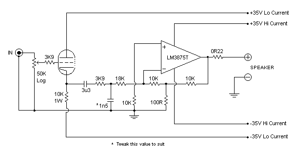
Hi Dsavidsk!
Very nice preamp! Could you tell us the specs?
Gain, output voltage, etc?
Tyimo
I use something similar for a DAC gain stage after a passive I/V.
Very nice preamp! Could you tell us the specs?
Gain, output voltage, etc?
Tyimo
Re: Time to decide what we want
Reasonable. I second
MIKET said:Design Goals:
1. Gain 20-40, this will alow a cd player to drive the MOSFET to full output.
2. Low output impedance. Wide Band performance.
3. Low parts count. We are using this to drive SEWA, otherwise would be wrong from a purist standpoint.
4. Output Swing 20V p-p minimum to assure we can get all 7 watts out of the MOSFET.
5. SE design no NFB.............thats my goal, but don't think it's unreasonable.
Those are my goals.......your thoughts
Reasonable. I second
Brian Beck said:I don’t see anything special happening at 3 volts, since the curve smoothly rises as you move left across the whole chart. If you limited the voltage swing, it certainly would reduce the distortion, the same as with almost any other distortion mechanism, but then you have a lower power amplifier. On another thread where a MOSFET was a driver and not the final stage, it was noted that when you bias these high voltage devices to closer to their maximum spec for Vds, the Crss drops in value and becomes more constant. But here a 200 Volt supply with 2 amps flowing wouldn’t work!
Oops, my mistake. Misplaced a zero. The steep uptick takes place around 30 volts for this FET. I have been looking at STB24F10 and STP20N20, where the Crss is pretty low and begins a steep rise arounng 3-5Volts. Sorry for the confusion. So for the Ir transistor, the input limiting strategy for a low power amp would be completely useless. For my application, I'm looking at a reflected impedence of the tube stage to be about 2K and the voltage at the FET's to be about 45V. So the Crss would be below 50 or so, until Vds dropped below about 3-4V, for a corner frequency of about 160K.
Sorry for the slightly off topic excursion.
Sheldon
1. Gain 20-40, this will alow a cd player to drive the MOSFET to full output.
My understanding of CD output levels are about 2 V RMS.
In my design notes, I assume a nominal 1 V RMS input, or about 3 V pp.
Given that, a minimum gain of 7 would give the 20V pp that is required.
I was doing a paper design inspired by your requirements:
CSS loaded ECC99 with an EDCOR 10k:600 interstage transformer parafead between Cathode and Plate (Anode).
Current tentatively set to about 10 Ma.
with a B+ of 240V, Plate Signal swing should be about 132 Vpp (6 Vpp input * mu 22), while output signal swing should be 1/4 of that, or about 33 Vpp. Output Z should be Rp/ 16, or 125 ohms.
Compromises:
Gain is a bit light for 1 Vrms, which "only" giving 16 Vpp.
The $12 EDCOR transformer is only good to 25 Vrms @ 30hz, which maxes out @ about 18 Vpp @ 30Hz
The 240V PS may be a culture shock for the intended audience.
I'll draw a schematic later today.
Any feedback welcome.
Doug
DougL said:
My understanding of CD output levels are about 2 V RMS.
In my design notes, I assume a nominal 1 V RMS input, or about 3 V pp.
Given that, a minimum gain of 7 would give the 20V pp that is required.
I was doing a paper design inspired by your requirements:
CSS loaded ECC99 with an EDCOR 10k:600 interstage transformer parafead between Cathode and Plate (Anode).
Current tentatively set to about 10 Ma.
with a B+ of 240V, Plate Signal swing should be about 132 Vpp (6 Vpp input * mu 22), while output signal swing should be 1/4 of that, or about 33 Vpp. Output Z should be Rp/ 16, or 125 ohms.
Compromises:
Gain is a bit light for 1 Vrms, which "only" giving 16 Vpp.
The $12 EDCOR transformer is only good to 25 Vrms @ 30hz, which maxes out @ about 18 Vpp @ 30Hz
The 240V PS may be a culture shock for the intended audience.
I'll draw a schematic later today.
Any feedback welcome.
Doug
hehe
my kind of preamp
- Status
- This old topic is closed. If you want to reopen this topic, contact a moderator using the "Report Post" button.
- Home
- Source & Line
- Analog Line Level
- Tube Pre Amplifier for SEWA 7 Watt ClassA MOSFET