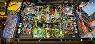
Upper left is a 12V 500mA standby supply that powers the board with the blue relay beside it - that makes touch power work. The larger SMPS in the middle is 12V for the heaters and the DC boost module (lower right) that generates -110V from 12V for the bias supply.
The lower right and left are the VA/PI/DR boards. The power supply boards are the ones with the big caps on them. One in the middle (RC filter), one off of the back (voltage dbl/quad - the main transformer is 120V but the working voltages are 320V and ~600V).
The lower right and left are the VA/PI/DR boards. The power supply boards are the ones with the big caps on them. One in the middle (RC filter), one off of the back (voltage dbl/quad - the main transformer is 120V but the working voltages are 320V and ~600V).
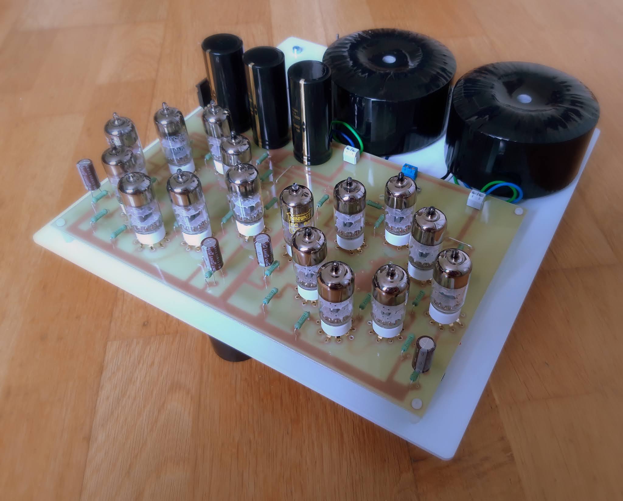
You're welcome. A picture is worth a thousand words, so I've annotated it. The RC filter in the middle is actually a CRC filter... but the first caps are in parallel with the last stage of the doubler. If anyone if wondering, the signal input is run using RG-174.
Attachments
Last edited:
L0rdGwyn nice work there,are they batteries at the front/underside? Also noticed how you mount the valve bases on their own sub assembly, that's a clever way of mounting them,any particular reason you do it that way?
Also another nice amp koda.
All your amps lads are an inspiration, keep em coming, Andy.
Also another nice amp koda.
All your amps lads are an inspiration, keep em coming, Andy.
Hi DA - thanks! And yup, those are batteries on the underside, the cathode voltage is jacked up in this design due to the feedback loop being buffered by a PMOS, so the grid voltage is also biased positive to offset it. Here is the amplifier circuit schematic.
.png")
There isn't much practical reason for the socket sub-assembly, really an aesthetic / design choice. A nice side effect though is it results in many points to mount terminal strips, so gave me a lot of flexibility in terms of component layout around the sockets.
There isn't much practical reason for the socket sub-assembly, really an aesthetic / design choice. A nice side effect though is it results in many points to mount terminal strips, so gave me a lot of flexibility in terms of component layout around the sockets.
L0rdGwyn,
On U2 tube, it appears you have a DC current sink in the cathode, and a current source in the plate circuit.
Is that correct?
If so, those will "fight" each other, and therefore the voltage across the tube might be different than you want.
Setting those two current sources to be exactly equal is a hard enough task.
Then just watch it go bad when the temperature changes, or the total voltage changes across the series circuit of the sink, U2, and plate's current source.
The above is just my opinion.
Last edited:
Hi 6A3 - M3 is not a current sink, it is a PMOS follower, buffering the feedback loop. The bias current is set by the LND150 CCS only.
The arrangement on the cathode was thought up by user SpreadSpectrum, here is the thread where he implemented it. He achieved some astonishing distortion results in his A2 circuit.
Corona: An Ultra-Low Distortion A2 DHT SE Amp Prototype
The arrangement on the cathode was thought up by user SpreadSpectrum, here is the thread where he implemented it. He achieved some astonishing distortion results in his A2 circuit.
Corona: An Ultra-Low Distortion A2 DHT SE Amp Prototype
However, the series differential will be critically dependent on M3's gate-to-source voltage at idle, and you may find you'll want an adjustable bias in place of the fixed battery bias. This kind of thing looks easier in simulation than in real parts.
All good fortune,
Chris
All good fortune,
Chris
Yes, bias is dependent on the gate-to-source voltage, which was investigated in prototype with real parts, as well as the voltage drop across R14. The PMOS parts are matched for gate-to-source voltage, so any variation in bias is from the tubes themselves. I prototyped with adjustable bias initially, decided on fixed battery bias. The 6F5 is a highly linear triode, with an active load variations in plate voltage as high as 50-75V do not significantly affect open loop gain between the two channels. Another builder might opt for adjustable bias, but I felt the added complexity was not worth the effort, just my preference. The completed circuit is in post #10389.
Member
Joined 2009
Paid Member
Hi 6A3 - M3 is not a current sink, it is a PMOS follower, buffering the feedback loop. The bias current is set by the LND150 CCS only.
The arrangement on the cathode was thought up by user SpreadSpectrum, here is the thread where he implemented it. He achieved some astonishing distortion results in his A2 circuit.
Corona: An Ultra-Low Distortion A2 DHT SE Amp Prototype
Interesting, the input stage is a hybrid Rush cascode.
That's a wonderful advantage we DIYers have over commercial production. If we're making only two channels of something, we need to make two the same, not gazillions. Exotics like series differential/ Rush cascodes become practical with a little elbow grease instead of cubic money.
All good fortune,
Chris
All good fortune,
Chris
")
Thanks.
Yes! Under the bed is where amplifiers go to die and be reborn. It's also general storage. I raised my bed on blocks to make some extra space. My place is only 35m³ (380 sqft).
There is even a complete KT88 amp under there but I can't be bothered buying a new set of KT88 and want to liquidate it instead. I'm stuck on trioded line tubes now.
Very nice indeed. But why do you call it a MA-1?A new MA-1 is taking shape.

- Home
- Amplifiers
- Tubes / Valves
- Photo Gallery