
I've been really interested in the hybrid world, but I can't find many designs out there that do what I want.
I've made a circuit layout of a basic tube driven mosfet amp that I found somewhere on the net. (please not it's not my design so I take no credit - only for the layout).
'As is' this circuit produces 50W into 8 ohms with a THD+noise of 0.64%, which doesn't seem too bad for a valve circuit considering most of this is second harmonic (softer on the ears).
If anyone thinks they may be able to improve upon the design (using bi-polar devices instead of MOSFETs in the output?) give it a go.
Thanks for looking folks!
Attachments
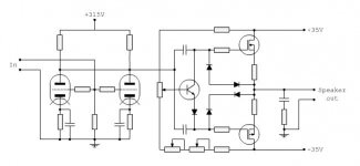
Hybrid amps
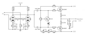
I have built similar circuits. The input tube is in parallel to increase the current available and to lower output impedance I guess.
The output stage you have seems to be a fairly easy load for one triode. If you want to raise the supply voltage (>35V) and want more power output , you would probably have to use a parallel stage as shown. The bias here is not particularly good as it would fluctuate with the supply voltage (on load) . Better to use zener stabilised voltage ( to the bias transistor) for this purpose. For a Hitachi type MOSFET you could use just a resistor instead of the transistor.
You should also note that you would have a fairly high output impedance with just two MOSFET's and no feedback. I found that the no feedback version sounds better than the one with feedback (which had lower measured distortion). So you could build what you have , it should be good. You can modify it later depending on what you think of its sound.
The high output impedance affects the bass end differently on different speakers. You should also remember that a high output impedance will result in a fluctuating frequency response at the speaker terminals due to the inherent variable impedance vs frequency of most speakers .
Build it anyway. It will be fun and is the road to greater fun.
The whole forum is here to help you along!
Cheers.
Bias point
I just noticed that you have some errors in the bias section. The bias transistor should go across the bias pot. Your diagram is wrongly connected. Also note that if the MOSFET's have internal protection zeners across gate and drain you only need an external resistor to protect it. Check it before adding more zeners.
I just noticed that you have some errors in the bias section. The bias transistor should go across the bias pot. Your diagram is wrongly connected. Also note that if the MOSFET's have internal protection zeners across gate and drain you only need an external resistor to protect it. Check it before adding more zeners.
Pathos amp
annex666,
recently listened to a Pathos amp, was just built like yours, sounded wonderful to me, very musical.
but, please. do not parallel tube sections, eats up detail resolution. Better use one tube for both channels, evcha section for one channel.
If chosen tube is not juicy enoug to drive the SS circuit, use a juicy tube (lower plate resistance, higher transconductance)
Thanks for the responce, but as I say the circuit is not my design.
If anyone wants to add pictures of improvements to the amp on this thread I would be more than happy to include them on the final design. Who knows maybe we'll end up with the "perfect" amp some day, lol.
Cheers for the input, keep it coming!

If anyone wants to add pictures of improvements to the amp on this thread I would be more than happy to include them on the final design. Who knows maybe we'll end up with the "perfect" amp some day, lol.
Cheers for the input, keep it coming!
OK, here's the circuit so far, I've added values and corrected some mitakes (it was quite late when I drew the original).
If anyone could design a better output stage then please feel free to post it or email it to me so I can incorporate it into the design. I don't really love the idea of MOSFETs.
Any feedback is good, keep it coming!
If anyone could design a better output stage then please feel free to post it or email it to me so I can incorporate it into the design. I don't really love the idea of MOSFETs.
Any feedback is good, keep it coming!
Attachments
Re: Hybrid amps
Thanks for the advice, but I'm quite new to electronics - I understand what you mean pretty much, but a diagram either posted on the thread or emailed to me would be a great help.
I'll incorporate any changes that are popular in the thread to the circuit (until it looses the nice neat simplicity - not to mention build-ability!)
Thanks to everyone who's been posting!

ashok said:I have built similar circuits... <BR>
...Better to use zener stabilised voltage ( to the bias transistor) for this purpose.
Thanks for the advice, but I'm quite new to electronics - I understand what you mean pretty much, but a diagram either posted on the thread or emailed to me would be a great help.
I'll incorporate any changes that are popular in the thread to the circuit (until it looses the nice neat simplicity - not to mention build-ability!)
Thanks to everyone who's been posting!
You may already have this, but a great web site for Valves and
Hybrid Amps is http://www.tubecad.com
In particular http://www.tubecad.com/april_may2001/2001_04-05.PDF and http://www.tubecad.com/articles_2002/Power_Buffers/Power_Buffers.pdf
I too am looking towards building a Hybrid amp, but using a BJT output stage.
Regards,
Tim
Hybrid Amps is http://www.tubecad.com
In particular http://www.tubecad.com/april_may2001/2001_04-05.PDF and http://www.tubecad.com/articles_2002/Power_Buffers/Power_Buffers.pdf
I too am looking towards building a Hybrid amp, but using a BJT output stage.
Regards,
Tim
For the hybrid amp,I would suggest not to use the pushpull output stage.Better drive the output trans with a single ended stage,with its own current source at V+ with same tube as signal.
I would try the Aleph current source with tubes (see http://www.passlabs.com on patents).I guess this would work perfectly,and better than the push_pull
I'd use some IRFP240 instead of the BUZ better sound I guess
I would try the Aleph current source with tubes (see http://www.passlabs.com on patents).I guess this would work perfectly,and better than the push_pull
I'd use some IRFP240 instead of the BUZ
better sound I guess
Annex666,
BUZ9xx are lateral Mosfets, designed specially for high quality audio, but with special characteristics. If the amplifier operates in class AB with 120 mA idle current, bias of gates must be constant (1.5 v or so between the gates) and needs no temperature compensation. If you use Vbe multiplier as shown in your diagram, crossover distortion will occur if the temperature raises...
If your amp is designed for pure class A operation, you have to experiment some *positive* temperature coefficient bias generator, in order to maintain the drain current approx. constant over the whole temperature range (25...125 °C). Or you have to tolerate that sound quality may vary, according to actual power output.
Regards, P.Lacombe.
Correct me if I'm wrong :
When using lateral and vertical type mosfets in output stages the Vbe multiplier is left off of the heatsink. This wasy it doesn't track the heat and just remains an amplified diode. Thus as the OPS heats up the transistor in the Vbe multiplier retains ambient temperature (I.E. not OPS temp) and consistant forward bias. In such a case, X-over distortion should not occur as the OPS heats up (and stabilizes). If using D-MOS such as the IRF devices, I think that the Vbe multiplier needs to be in contact with the heat sink as would BJT's to prevent thermal runaway.
I've seen many schematics that use both M and V - MOS with a Vbe multiplier, but generally there is little documentation of heatsinking. I guess most designers are well versed in the subject and assume the same of anyone reading the schematic.
It should also be noted that different MOSFETs will require different voltage biases. The Lateral types needing the least amount with the IRF types needing the most. The V types seem to be in the middle, tho closer to the L types.
I like the idea of using a Vbe multipier as this gives MUCH more contral over the biasing than using any sort of diode. I also think that it sounds better because of this control.
-D.
- Status
- This old topic is closed. If you want to reopen this topic, contact a moderator using the "Report Post" button.
- Home
- Amplifiers
- Tubes / Valves
- The best of both worlds?