I just posted this over on the solid state forum in a thread on low feedback amplifiers. Thought it might be of interest here too. This is a tube output stage idea based on M. Hawksfords error correcting output stage. (M. Hawksford JAES, Vol 29, Jan/Feb 1981 pp 27-31 on the web too at: http://wes.feec.vutbr.cz/~gratz/Download/Hawksford.ZIP )
I have fitted the Hawksford idea to a partial cathode feedback circlotron output stage ( or "Elliptron") but it can be easiliy adapted to any P-P (or even SE for that matter) output:
I have fitted the Hawksford idea to a partial cathode feedback circlotron output stage ( or "Elliptron") but it can be easiliy adapted to any P-P (or even SE for that matter) output:
Attachments
Hi Smoky,
I am very interested in the Hawksford stuff at the moment, I'm working on an output stage with that applied. As you surely know, the big difference between 'normal' feedback and the Hawksford error correction (which is of course also a form of feedback) is that with 'normal' feedback we try to maximize loop gain to have as much feedback gain as possible. With the Hawksford topology, the part of the output that is fed back is ideally exact 1. You take the difference between the stage's input and output, and that is exactly what you add to the input to make the stage gain perfectly 1. That is also why Hawksford says that basically it is only useful in stages that are already close to a gain of 1, like EF output stages in SS amps.
So, after this long (for me) ramble, how do you do this? Not being a tube guy, I'm not familiar with the gain levels etc in output stages. Do I get it correctly that you take the signal part from the 's' tap and then return it in the correct ratio via the R1 resistive divider?
Jan Didden
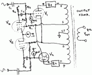
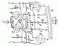
How it works
Basic operation is as follows. V1 and V2 are the normal output tubes in circlotron-like configuration. (The screen taps on the transformer are used for the cathode connections here to reduce the amount of grid drive compared to a full circlotron connection.)
In normal operation, the cathodes of V1 and V2 will behave as cathode followers with the plates driving the other section of the transformer. The cathodes will have signals slightly less than their respective grids due to the grid-cathode drive signal required to enable current flow. So, depending on V1,V2 transconductance and load impedance, the cathodes will have a slightly reduced, say 90%, replica of the grid drive signals.
Now we add V10,V11 for error correction. The resistors R1 and R2 monitor the input V1 grid drive signal and an inverted replica of the cathode signal. They are proprtioned in such a way so that if the cathode is properly following %90 of the V1 grid drive, then no signal appears at the V10 grid and no action is taken. If however the cathode is not correctly producing %90 percent of the V1 grid drive (load impedance variation, crossover dist. in class AB, etc...) , then a correcting signal is produced on the V10 plate. Resistors R3 and R4 are sized so as to just produce unity correction gain. Likewize, V11 corrects V2 operation in a symmetric manner.
When tuned up correctly for unity correction gain, variation of the output impedance has no effect on output signal. A simple way to align/test this is connecting another power amplifier output thru an 8 Ohm power resistor to this amplifiers output and putting a square wave signal into the other amplifier. R3, R4 (and the V11 resistors) are tweeked until no square wave signal appears on the V1,V2 cathodes or plates.
Don (of course, if you don't get it right, you may get lots of SMOKE!
 )
)
Hi Jan,
I just saw your post as I was about to post this. Yes, I just use the cathode follower portion of the signal for the error monitoring, so is close to unity gain.
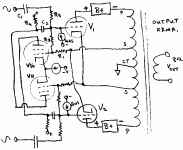
Basic operation is as follows. V1 and V2 are the normal output tubes in circlotron-like configuration. (The screen taps on the transformer are used for the cathode connections here to reduce the amount of grid drive compared to a full circlotron connection.)
In normal operation, the cathodes of V1 and V2 will behave as cathode followers with the plates driving the other section of the transformer. The cathodes will have signals slightly less than their respective grids due to the grid-cathode drive signal required to enable current flow. So, depending on V1,V2 transconductance and load impedance, the cathodes will have a slightly reduced, say 90%, replica of the grid drive signals.
Now we add V10,V11 for error correction. The resistors R1 and R2 monitor the input V1 grid drive signal and an inverted replica of the cathode signal. They are proprtioned in such a way so that if the cathode is properly following %90 of the V1 grid drive, then no signal appears at the V10 grid and no action is taken. If however the cathode is not correctly producing %90 percent of the V1 grid drive (load impedance variation, crossover dist. in class AB, etc...) , then a correcting signal is produced on the V10 plate. Resistors R3 and R4 are sized so as to just produce unity correction gain. Likewize, V11 corrects V2 operation in a symmetric manner.
When tuned up correctly for unity correction gain, variation of the output impedance has no effect on output signal. A simple way to align/test this is connecting another power amplifier output thru an 8 Ohm power resistor to this amplifiers output and putting a square wave signal into the other amplifier. R3, R4 (and the V11 resistors) are tweeked until no square wave signal appears on the V1,V2 cathodes or plates.
Don (of course, if you don't get it right, you may get lots of SMOKE!
)Hi Jan,
I just saw your post as I was about to post this. Yes, I just use the cathode follower portion of the signal for the error monitoring, so is close to unity gain.
Got it. I think. Wil print the schematic and study it.
Interestingly, my very first amp I built when working for Philips in the 60-ies (my second name is Methusalem). That was.. a circlotron with 2 times 807 tubes. Of course, working for Philips made it easy to get those power transformers with 3 separate hv supply windings.
This amp was OTL for the 800-ohms speakers Philips was pushing at that time for the purpose (the fabulous 9710-series). As soon as the first power transistors (OC29) came out we salivated over them and forget all about tubes. Sigh.
Jan Didden
Hi Jan,
I guess I neglected to mention on this thread that I haven't actually built this yet! So don't take it as gospel for a working design. Will try it out soon though.
I have a modified version/idea of the circlotron/elliptron which uses just a single power supply too, but have yet too try it out, the parts are sitting ready on the bench collecting dust so far:
http://www.diyaudio.com/forums/showthread.php?threadid=19624&highlight=
http://www.diyaudio.com/forums/showthread.php?s=&threadid=32852&highlight=
Don
design limitations
The error monitoring points come from the opposite "S" ( ultra-linear Screen taps) tap on the Xfmr. to the applicable cathode, in order to get an inverted cathode signal, and so depends on the Xfmr. having good coupling between the "S" taps. (At least each output tube IS driving current through BOTH "S" to "CT" to "S" sections, so first order coupling should be good, we're not talking an isolated secondary here.) This limitation may require some bandwidth limiting in the error correction circuit to prevent phase shift or oscillation at high frequency. The present circuit does however use BOTH the direct cathode signal AND the opposite "S" tap signal simultaneously, due to its symmety, to form its output. ( due to the differencing action of the LTP) So any small phase difference (besides the expected 180 degrees) between the "S"s is diluted.
The Hammond 1650T Xfmr. that I am using for the circlotron/elliptron output has the "S" to "S" section wound on the core as a single interleave section so should be pretty good. But until I construct this, I won't know how well this works. If this proves to be a serious problem, then I may have to re-configure the V10/V11 diff. amp. connections to work with the direct, non-inverted, cathode signals only. Probably can not still be done for both output tubes using the same diff. (LTP) amp. though.
Don
further iterations
Just some notes and further thoughts.
The signal sources driving C1 and C1' inputs (in solid state designs anyway) are usually low impedance (emitter followers, cathode followers or low Rp triode here). But I think Jarek's design (in the SS thread on no feedback designs) has shown that this is not necessary, but does make calculating parts values for unity gain a bit more difficult. However, depending on the previous stages output impedance significantly for gain setting, instead of on R3 (and other factors), opens one to the problem of varying plate resistance of the previous driver tube with signal level (particularly for triode plate output drivers). So unity feedback gain may only exist at one signal level.
It may be helpful to put a resistor in series with C2 and C2' and /or use degeneration resistors in the LTP (V10 & V11) cathodes to adjust feedback gain. One would like to maximize the value of R4 (and R4') so as to minimize loading on the previous driver tube providing the signal to C1 ( &C1' ). Likewise, R2 and R1 (& R2' and R1' ) would like to be high resistance to minimize driver loading. Here, its just the ratio that matters fortunately as long as V10 (& V11) maximum grid leak impedance is not exceeded. May be some noise considerations too for very high resistance values. I'm sure actual construction of this circuit idea will find some more useful mods too.
By the way, the input driving signals to C1 (& C1' )must be from a class A stage (ie, 100% duty cycle) rather than from a class B driver. The V10, V11 LTP requires balanced inputs of 100% duty cycle to perform its function correctly. The output stage, V1 and V2 however can be Class AB or Class A (determined by grid bias level).
Don
Oops! a few clarifications
After getting a good nights sleep and reviewing what I posted yesterday, I see some things I need to correct.
The ratio of R1 to R2 sets the nominal gain expected at the cathode point (relative to the V1/V2 grid drive signals) as mentioned, typically something like 90% or 0.9 gain for a cathode follower. One wants to set this at the nominal gain of the output tube cathode into the reflected load impedance, so that the error correction circuitry is normally passive. The error correction circuitry should only be actively modifiying the drive level when deviation from the norm is occuring. (due to speaker impedance variation, crossover distortion, etc...)
The gain of V10 loaded by R3, R4 and the output Rp of the preceding driver tube (likewise for V11 ....) sets the maximum OPEN loop gain (for the error correction feedback loop). Not a unity gain as I had suggested before. Higher open loop gain enables the circuit to approach unity (well, er, 0.9 gain in this case) CLOSED loop gain more ACCURATELY.
Deviation of the Rp of the preceding driver tube could then influence the open loop gain if R3 does not dominate, but would only indirectly have a smaller influence on the accuracy of closed loop gain. Deviation of the open loop gain could however influence stablility of the error feedback loop if the phase margin of the loop is low. Possibly causing oscillation bursts at signal peaks.
For this reason, one wants to set the nominal error corr. loop gain at a safe level, and a resistor in series with C2 (and C2' ) or cathode degeneration resistors for V10/V11 may be useful if needed to lower gain.
Also, for the two amplifiers connected by an 8 Ohm power resistor test, one would be adjusting the R1/R2 (and R1'/R2' ) ratios, (not R3 and R4 as suggested earlier) to minimize feedthru of the square wave from the 2nd amplifier. Hope I got it right this time!
Don
Re: clarification
My previous post #8 timed out while I was editing it and it has several mistakes, so please disregard # 8. (the open loop/ closed loop talk in post #8 only applies if the boost signal is applied in a way that does not affect the reference input for grid drive level, just the actual applied grid drive, and is a different scheme from the Hawksford style design considered here) Here is the correctly edited version:
The ratio of R1 to R2 sets the nominal gain expected at the cathode point (relative to the V1/V2 grid drive signals) as mentioned, typically something like 90% or 0.9 gain for a cathode follower. One wants to set this at the nominal gain of the output tube cathode into the reflected load impedance, so that the error correction circuitry is normally passive. The error correction circuitry should only be actively modifiying the drive level when deviation from the norm is occuring. (due to speaker impedance variation, crossover distortion, etc...)
The gain of V10 loaded by R3, R4 and the output Rp of the preceding driver tube (likewise for V11 ....) sets the error loop gain (for the error correction feedback loop). This error correction gain needs to be UNITY so that the V1 ( and V2) drive input signals are only boosted enough to correct the deficiency and no more. The unity error loop gain and the forward cathode follower gain (0.9 here) are distinctly different entities.
Deviation of the Rp of the preceding driver tube could then influence the error loop gain if R3 does not dominate. Deviation of the error loop gain could also influence stablility of the error feedback loop if the phase margin of the loop is low. Possibly causing oscillation bursts at signal peaks. But the main effect of deviation from unity error loop gain would be to allow distortion thru (or even generate distortion if > 1).
For this reason, one wants to set the nominal error corr. loop gain accurately at the unity level (adjusting for minimum feedthru using the two amplifier test with connecting 8 Ohm resistor and square wave signal). A resistor in series with C2 (and C2' ) or cathode degeneration resistors for V10/V11 may be useful if needed to lower gain. Some frequency dependant rolloff of the error corr. gain may be necessary if phase margin (mainly of "S" to "S" in the Xfmr.) is a problem at high frequency.
Hope I got it right this time!
Hi,
Interesting stuff....
It looks like a double bootstrap to me, first around the phase splitter, second one around the cathode feedback.
If this works, wouldn't it also work with the B+ connected to the CT iso of the dual PS?
I could of course be wrong, haven't read all the docs yet.
Cheers,
Interesting stuff....
It looks like a double bootstrap to me, first around the phase splitter, second one around the cathode feedback.
If this works, wouldn't it also work with the B+ connected to the CT iso of the dual PS?
I could of course be wrong, haven't read all the docs yet.
Cheers,
Conventional P-P output
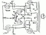
Hi Frank,
I just did a little thinking about applying the Hawksford scheme to a conventional P-P output stage and have some diagrams to post. However, I am finding it problematic for the conventional P-P output with center tapped output xfmr. The problem is with using the xfmr. to get an inverted signal from the tube being actively corrected. For an ideal xfmr. (or simulation) it works, but for a real design probably not so well, since the opposite winding is idled (in class AB, and the whole point is to get class AB gain cleaned up so it looks like constant gain class A). (The circlotron/elliptron had the advantage of each of the output tubes always driving both of the cathode follower xfmr windings simultaneously.) Maybe, a low leakage inductance toroidal output could be made to work.
1st diagram is just a slight mod to apply this to a partial cathode drive output or McIntosh output. The McIntosh, with its bifilar xfmr windings, probably will work OK. Notice that I have used a pentode driver and combined R3 as load resistor for both Vdriver and V10. With high Rp pentodes, R3 will dominate the impedance at the feedback sumation point and hold loop gain steady I think. The 2nd diagram (next post) is for a conventional P-P CT'd output. It would require higher value R1's and some fix-ups for bias.
Attachments
here is the conventional P-P stage:
(if the drive signals do not come from a high Rp pentode pair, as in the last diagram, then probably would need to use a cathode follower with a series output resistor to set a constant and defined impedance for the loop summation points)
(if the drive signals do not come from a high Rp pentode pair, as in the last diagram, then probably would need to use a cathode follower with a series output resistor to set a constant and defined impedance for the loop summation points)
Attachments
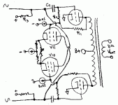
Single power supply Elliptron with Hawksford corr. ckt.
The whole Shebang ( I will try to throw this together soon with a pentode LTP driver/splitter ahead of this, we'll see if this really all works! ):
T1: Hammond 1650T (28% cathode drive using 40% UL taps)
L1: dual 240V primary 60 Hz utility xfmr.
V1,V2: 6HJ5 beam pentodes (could use triodes )
V10,V11: 6J11 or 6BN11 dual pentode
Attachments
Hi,
Don,
While I think it will definetely improve the distortion figures, I have my reservations about doing away with the class x-over distortion altogether.
Anyway, if you have the iron for it it may well be worth a try.
Cheers,
Don,
The whole Shebang ( I will try to throw this together soon with a pentode LTP driver/splitter ahead of this, we'll see if this really all works! ):
While I think it will definetely improve the distortion figures, I have my reservations about doing away with the class x-over distortion altogether.
Anyway, if you have the iron for it it may well be worth a try.
Cheers,
lunatic - fringe extension to circuit
I just had another idea. Since the gain required of V10/V11 is quite low for unity error loop gain, I could use G2, screen grid control, with them for the R1 inputs instead of G1 control. (R2 inputs would stay on G1's) This would make for easier connections to B+ level type voltages in the circuit, ie. the R1 's in the circuit could connect directly from G2 to the "S" points (maybe a 50% resistive divider to get a lower idle screen voltage level) on the output xfmr, instead of to the L1 inductor (eliminates the Ck's in series for a cleaner signal and gets rid of a floating screen supply voltage too). Since the G1 inputs have higher gm than the g2 inputs, R2 resistors would be pushed up to nice high values to get a resultant null for 0.9 cathode follower gain set point. ( I know, pushing my luck here. But just think, NO ONE will EVER be able to figure out how this circuit works! or even, what it does! can pull V10/V11 out and it still works!! )
 Don
Don
I just had another idea. Since the gain required of V10/V11 is quite low for unity error loop gain, I could use G2, screen grid control, with them for the R1 inputs instead of G1 control. (R2 inputs would stay on G1's) This would make for easier connections to B+ level type voltages in the circuit, ie. the R1 's in the circuit could connect directly from G2 to the "S" points (maybe a 50% resistive divider to get a lower idle screen voltage level) on the output xfmr, instead of to the L1 inductor (eliminates the Ck's in series for a cleaner signal and gets rid of a floating screen supply voltage too). Since the G1 inputs have higher gm than the g2 inputs, R2 resistors would be pushed up to nice high values to get a resultant null for 0.9 cathode follower gain set point. ( I know, pushing my luck here. But just think, NO ONE will EVER be able to figure out how this circuit works! or even, what it does! can pull V10/V11 out and it still works!! )
Don- Status
- This old topic is closed. If you want to reopen this topic, contact a moderator using the "Report Post" button.
- Home
- Amplifiers
- Tubes / Valves
- Hawksford style error correcting output