I've used the simple no-feedback source follower to set B+ in circuits in the past, but it is preceded or followed by additional filtering.
Preceding the source follower there will be a choke input filter using 10H choke and either 47uF, 100uF, or 800uF (!!) caps, since I have them.
Question: How much capacitance can be used after the psu source follower? I have film caps at suitable working voltage from low values all the way up to 24uF. Can too much capacitance on the source cause a current spike or 'kickback' of some kind?
I like to add some visual interest to a PSU occasionally, hence the original FET+VR circuit.
Elvee's circuit works with that same combination of 15V zener and 0D3, so I might give it a go sometime. It should be useful for a phono preamp using high gm tubes, right?
--
It will do the job for sure, but it will have a lower performance than the circuit I proposed: a bit more than twice the residual ripple, which is anecdotal in the grand scheme of things, but also an output impedance of ~15Ω, which is about 200 times the 0.08Ω you could expect, very much less anecdotal, maybe enough to disturb the zenitude of even the most fatalistics.I'm curious whether this simple source follower will do the job. If not, I can convert to the circuit you recommended earlier (see first attached schematic).
That's for you to decide, of course.
In case you choose the more picturesque option, I'd recommend you ditch the 0.1µF across the VR tube: it will only serve to unnerve it without serving any useful purpose, because you have the 2.2µF across the whole ref string, which will be more effective due to the dynamic resistance of the zener, and anyway, no noise will manage through R15/C9.
Sorry if this no-nonsense approach is disturbing to some, I know that valve-lovers love to concentrate on minor, non-operational issues, but I don't adhere to the same folklore: I just make things as effective as materially possible
I'll have to build one of the circuit you posted, I'm pretty happy with a basic source follower type with the "enhancements" I mentioned, but for higher current use the lower source impedance and higher PSRR sounds interesting. I've got some mosfet capacitance multiplier boards with Zener reference to build up, so it would be neat to compare.
It will do the job for sure, but it will have a lower performance than the circuit I proposed: a bit more than twice the residual ripple, which is anecdotal in the grand scheme of things, but also an output impedance of ~15Ω, which is about 200 times the 0.08Ω you could expect, very much less anecdotal, maybe enough to disturb the zenitude of even the most fatalistics.
That's for you to decide, of course.

Yeah, my zenitude is definitely disturbed NOW!
Well okay... if I attempt making the MOSFET based version of your series regulator, I'd want to try it with the 15V zener and 0D3 VR tube reference included for its picturesque qualities. So, I'd have some questions. Like for instance:
- Would a 2.2uF cap across the zener and VR tube be enough bypassing there?
- Is there a better part to use for the error amp than a DN2540 (M2)? LND150, perhaps?
In case you choose the more picturesque option, I'd recommend you ditch the 0.1µF across the VR tube: it will only serve to unnerve it without serving any useful purpose, because you have the 2.2µF across the whole ref string, which will be more effective due to the dynamic resistance of the zener, and anyway, no noise will manage through R15/C9.
Sorry if this no-nonsense approach is disturbing to some, I know that valve-lovers love to concentrate on minor, non-operational issues, but I don't adhere to the same folklore: I just make things as effective as materially possible
Not at all disturbing. In fact, very helpful.
Now I'll have to sit with my perfboard and figure out a layout for your circuit.
Last edited:
Question: How much capacitance can be used after the psu source follower? I have film caps at suitable working voltage from low values all the way up to 24uF.
You should be fine with modest film caps. I've used 2-10uF on this kind of circuit in the past. With a CRC you can add a lot more capacitance (but lose some voltage and regulation).
Elvee's circuit works with that same combination of 15V zener and 0D3, so I might give it a go sometime. It should be useful for a phono preamp using high gm tubes, right?
--
Yeah, for phono I'd do a feedback regulator like what Elvee proposes. I have done a stout filter and simple VR shunt for phono, but that is limited on current and takes up a lot of real estate.
I don't think you're disturbing anyone Elvee! Great points and suggestions. In DIY, there's value in both high performance and easy-to-grasp circuits.
There doesn't seem to be any drawback to increasing capacitance arbitrarily, even if that capacitance looks theoretically perfect, but this needs to be tested in real life: there are sometimes completely unexpected effects coming into playQuestion: How much capacitance can be used after the psu source follower? I have film caps at suitable working voltage from low values all the way up to 24uF. Can too much capacitance on the source cause a current spike or 'kickback' of some kind?
Be careful, my circuit is a true regulator (ie. DC amplifier), and its gain is calculated to transform the 150V tube ref voltage into ~165V, so no zener is necessary.Elvee's circuit works with that same combination of 15V zener and 0D3, so I might give it a go sometime. It should be useful for a phono preamp using high gm tubes, right?
It might work as unity gain buffer, but I cannot answer that directly, it will have to wait tomorrow
--
As I said, the VR tube is on its own, and bypassing it directly with 2.2µF will certainly make it oscillate.- Would a 2.2uF cap across the zener and VR tube be enough bypassing there?
If you want some kind of bypass anyway, you would need to add some series impedance, but it will degrade the static regulation.
Maybe an inductor? It could make matters much worse -or not-, maybe some members have experimented in this direction?
Anyway, as VR tubes didn't tolerate parallel capacitance, they were designed to have a low intrinsic noise
The key parameter in this case is the forward transconductance: 325mA/V for the 2540 against 2mA/V for the LND150, so it's a no brainer, but you can certainly find small MOSfets having a higher Gfs than the 2540, including enhancement types: the circuit will work indifferently with both varieties- Is there a better part to use for the error amp than a DN2540 (M2)? LND150, perhaps?
Not at all disturbing. In fact, very helpful.
Now I'll have to sit with my perfboard and figure out a layout for your circuit.
OK, here's a stab at adapting the feedback (series) regulator. Attached schematic. I took a quick read through the thread about high voltage regulators and tried to apply the protection parts from there. I'm not sure about R16 (2.2R) or D5 (1N4004 from drain to source of M2). Otherwise I just added two 15V zeners from gate to source of the two IRF820s.
R1 and R2 values needed to be adjusted for 162V out. I suppose a pot there would make the regulator adjustable. Maybe a 25k pot so that I can fine-tune it on test?
I expect I've missed something, or goofed something up...
R1 and R2 values needed to be adjusted for 162V out. I suppose a pot there would make the regulator adjustable. Maybe a 25k pot so that I can fine-tune it on test?
I expect I've missed something, or goofed something up...
Attachments
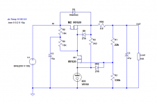
As drawn, R16 serves no purpose, it waste a bit of heat and slightly increase the output resistance, but fundamentally it poses no problem.OK, here's a stab at adapting the feedback (series) regulator. Attached schematic. I took a quick read through the thread about high voltage regulators and tried to apply the protection parts from there. I'm not sure about R16 (2.2R) or D5 (1N4004 from drain to source of M2). Otherwise I just added two 15V zeners from gate to source of the two IRF820s. .
Using it for protection would make it useful: either with the cathode of D9 returned to output, and values adapted, or with a small sensing transistor.
The latter has my preference, because it is minimally intrusive
Yes, place a 10 or 22K trimpot at the junction of R1 R2, wiper to the gate of M1.R1 and R2 values needed to be adjusted for 162V out. I suppose a pot there would make the regulator adjustable. Maybe a 25k pot so that I can fine-tune it on test?
D5 is redundant, because it is in parallel with the much larger body diode of the MOS.... but it does no harm.I expect I've missed something, or goofed something up..
Otherwise, the circuit looks OK.
If one wanted to convert the regulator to true unity gain, that wouldn't be possible without resorting to additional translations, not attractive.
However, if a residual gain of 1~2% beyond unity can be tolerated, the problem very much simplifies itself:
The two traces show the output and refence voltages: it is minimal.
The bias of the VR tube with a resistor is no longer possible, so R8 and R9 have been reduced to make up for the missing current.
Attachments
Do you mean does the VR tube ignite in that circuit?
(Good question...)
I guess it would be pretty easy to take voltage from either before or after M2, send it through an appropriately sized resistor, to the plate of the 0D3, to make sure it has the correct current going through it, and starts with a high enough voltage on its plate for ignition.
How about taking it from before M2, which is at about 205V. 4.7k 2W from there to the 0D3 plate would drop 55V, or 11.7mA. That should do it, right?
Last edited:
With the series feedback regulator, is it normal to have some high frequency hash showing up on the power supply rail coming from the voltage reference? It seems to appear in the simulation whether I use zener diodes or I use an 0A2 (Stephie Bench's model).
I've attached the .asc and the 12HL7, potentiometer and 0A2 model files so you can see what I'm seeing, or if you feel so inclined, correct it.
I've attached the .asc and the 12HL7, potentiometer and 0A2 model files so you can see what I'm seeing, or if you feel so inclined, correct it.
Attachments
several volts of movement under load at < 5hz will not be audible. It is the ripple rejection that is most important. I've got -112 db ripple rejection from several capacitors and a 2N5551. This also guarantees great voltage stability as if running off batteries.
My phono preamp has 3 stage ripple removal on 18 volt rails.
My phono preamp has 3 stage ripple removal on 18 volt rails.
Last edited:
Could you zoom on it and post the resulting picture, just to make sure we are talking about the same thing, and not an extraneous artifact?With the series feedback regulator, is it normal to have some high frequency hash showing up on the power supply rail coming from the voltage reference?
Good thinking! I should have posted about this earlier. I'm working on the thing today, and realized just a little while ago that the 'high frequency' I saw was actually that 1kHz sine wave (audio test signal) I was feeding into the grid of the 12HL7 tube. Just like you said in the earlier post. It's so tiny I thought it was some kind of high frequency riding on top of the DC. It's not.
This simple regulator looks excellent for this application (in simulation). The one and only downside I can see is that the pass MOSFET (M2) will need a decent heatsink. I'm going to put a series RC after the LC, preceding the two channels' regulators. I have some 220R 10W, so I can use one of them and maybe a 450uF 400V capacitor I have waiting for use. That should knock the raw supply down to about +180V, so the pass MOSFETs will only dissipate 1.5W each. That will be much easier to heatsink.
How hot do those MOSFETs get at startup? If quiescent dissipation is 1.5W, how much hotter are they likely to get for the few seconds before the tube starts drawing full plate current?
_____________________________________
With a 10k resistor (unbypassed) stuck in the cathode of the 12HL7, so that the tube only draws 0.5mA plate current, and with the full +325V input voltage I'd get from cap-input power supply, the regulated output is still close to 160V and M2 is dissipating 1.6W.
But if I increase the source voltage (from the rectifier) to +325V, and with the 12HL7 drawing full current (worst case scenario), M2 dissipates almost 8W. Does that mean that if I use a large clip-on heatsink that is rated to safely dissipate up to 4W of heat, that the pass MOSFET will still fry on turn-on, while trying to dissipate 8W for half a second?
Last edited:
8W for half a second is 4J, ~=1 cal, almost certainly not enough to raise the temp to dangerous levels, even ignoring the heatsink.But if I increase the source voltage (from the rectifier) to +325V, and with the 12HL7 drawing full current (worst case scenario), M2 dissipates almost 8W. Does that mean that if I use a large clip-on heatsink that is rated to safely dissipate up to 4W of heat, that the pass MOSFET will still fry on turn-on, while trying to dissipate 8W for half a second?
Of course, one would need to make the complete calculations using thermal capacities, etc. to be positively certain, but that's just a standard precaution and things should work out OK
I hope it's OK if I pester you with a couple more questions...
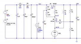
Referring to the attached schematic:
1) I got confused between my original circuit and your modification for more feedback/lower gain, and I wired in 4.7k ohm resistors for R4 and R5 (they're 15k in the previous schematic) but left in R3 (the current setting resistor for the VR tube). In simulation the only difference I see is about 1.5mA more current drawn by M1 and the VR tube, but no change in performance. Do you see a problem there?
2) Assuming R4 and R5 being 4.7k ohms is OK, what pole is acceptable for the low pass filter formed by R4 and C3? That looks like a decoupling network for M1, with R5 as the drain load resistor. Am I close?
If that is the case, then we'd want R4/C3 to attenuate frequencies down as low as possible. If I'm using 4.7k for R4, do I want to use at least 22uF or 33uF for C3? Or would 10uF still be OK there?
3) What value of capacitor is appropriate for C4 (shunting the regulator's output)? Would 10uF be fine there? Or do we want more, like 47uF?
Would making C4 a film capacitor be beneficial? If so, what value cap is too small?
4) As you can see, I removed R16, and I've left out the diodes D5, D9 and D10 from the previous schematic.
--
Attachments
Last edited:
- Status
- This old topic is closed. If you want to reopen this topic, contact a moderator using the "Report Post" button.
- Home
- Amplifiers
- Tubes / Valves
- +150V DC Vacuum Tube Regulated Power Supply?