Also, GoatGuy, check your PM inbox lol
LOL - OK, I will.
But in the meantime … shouldn't the cathode-ring of D3 and D2 be reversed? I would think you're trying for a full-wave bridge. (Actually, without their legend reversal, this is a "do nothing" circuit.) … just saying.
Also, it looks like you've shown both sides in the upper drawing (blue & red), but only one side (red) in the lower graphic. No worries… we "get it", I'd guess.
PRETTY SWEET layout. Might I suggest … "since its free", that the yellow colored legend layer also have "VAC-IN" on the left connector and V+ on U₃, and V- on U₂. Its free.
GoatGuy
Right, I was referring to replacing R2 but maintaining the MOSFET pass device.
I tried that too. In simulation it made zero difference.
Lingwendil's board looks good too. I recently made some boards that use an LR8 in place of the zener string (yet to stuff and test though). Only problem is these don't glow")
Yeah, and I'd have to buy stuff, too. This is a definite junkbox project.
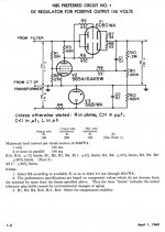
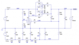
That National Bureau of Standards Preferred Circuits book that Merlin suggested has a nice circuit, the NBS Preferred Circuit No. 1. I altered it a little to use 6AC7 and 0D3, by changing the -150V negative supply to -225V. I also had to futz with some resistor values, but I think I got it.
With a 100mA load and the 100k adjustment pot set to 50%, the output voltage is +168V. That's fine. Adjustment range is from 152V to 182V. Ripple attenuation is about -70dB. It looks pretty OK.
I need to check out GoatGuy's refinements to that MOSFET-0D3 circuit you suggested. That's a lot simpler.
--
Attachments
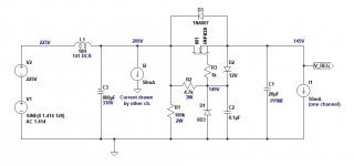
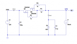
Here's circuit I'd use, incorporating the advice, and showing markedly improved ripple rejection.
Thanks. That really does look like a winner. Kinda nice that it's a collaborative effort.
I changed a couple things.
- Changing R1 to 47k makes a 3W part necessary. If I have one, I'll do it. But I know I have some 100k 2W. Changing the values around doesn't seem to change things very much. Why did you want to see more current going through R1?
- If R2 is changed to 10k, the output voltage goes down to 142V, because the 0D3's voltage dips with less current through it. The sim says an R2 of 4.7k gets the 0D3 to draw about 12.5mA, and output voltage rises to 145V. I guess that 3V won't matter. This will need to be sorted out if/when built.
- I added a gate protection zener (12V).
- For R0, a 1k resistor with 110mA through it would dissipate 12W, which is way more heat than I want to deal with. Instead, I substituted a 10H choke with 141 ohm DCR I have on hand. If C1 is 100uF, LTspice says there will be a low-Q +5dB resonance centered around 5Hz. I have some 800uF 330V caps, so I put that in for C1. The resonance was completely smoothed out, and ripple is reduced a lot. What I don't know is what that high a capacitance will do at turn on. It'll make for quite a surge, I'm sure. If I blow rectifier diodes, then I'll swap in a smaller value.
- With all that filtering before the stabilizer, it doesn't make much difference what value is chosen for C3. Since I have some 20uF 400V metalized polypropylene caps, I figure this would be a good place to use one. The ESR of the film cap will be very low.
With all that in place, LTspice says ripple rejection will be on the order of -95dB. That's crazy good. Schematic attached.
--
Attachments
... Hey Merlin! That's very helpful indeed. Preferred Circuit No. 1 fills the bill. The only problem is the need for that negative supply...
The negative supply is not essential. If you are an experienced circuit-bender you can re-rig without it.
Did you put the diode the wrong way ? Or has it to much leaking current ?oops. Mistake in that last schematic. The zener diode D2 destroys it. Take that out.
With D2 from gate-source of the MOSFET, the output voltage drops to 86V.
I don't know why it does that. I don't understand...
Originally Posted by rongon

... Hey Merlin! That's very helpful indeed. Preferred Circuit No. 1 fills the bill. The only problem is the need for that negative supply...
Perhaps try it this way
Mona
Attachments
oops.
It's working.
But... output impedance below 5kHz is over 1 Ohm!
10kHz 0.7 Ohm
100kHz 0.08 Ohm
Attachments
It's working. ... But... output impedance below 5kHz is over 1 Ohm! ....
Of course. It is a cathode- (source-) follower with no error amplifier. The true Z out will be the cathode (source) impedance. Which *varies* with device current. And at 50mA, probably several Ohms.
Here this device impedance is swamped by 20uFd, which is why you have Zout as low as you do.
Note that (without a cap) the Zout is true only for the device passing current, pull-up. If the load "kicks back", device current goes to zero and device Zout goes to infinity.
Thanks for your input everyone. Okay, about that simple source follower...
If the usage is in a stereo headphone amplifier, with a pair of triodes run as common cathode amplifiers loaded by output transformers, the load on this simple source follower/voltage stabilizer would be pretty much constant... Correct?
If the load (current draw) is constant, then under what circumstance would the load "kick back"?
--
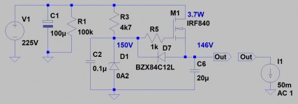
Maybe a CCS feeding the VR is worth a sim?
Tried it. It looks like its ripple rejection would be about -40dB, since you can't put a large value capacitor in parallel with the 0D3, which is on the DC output. A C-R-C filter in front of it would make things work.
My only complaint is that M1, the upper MOSFET in the cascode CCS, will dissipate 5W and so will need some kind of heatsink. Minor problem. I have some screw-on, freestanding heatsinks, sort of like the clip-on ones but larger, meant to stand up in free air (not affixed to the chassis). I think that would be okay for dissipating 5W.
Also, I worry that the 0D3 would pass too much current at turn-on. With 10mA drawn by the load, the 0D3 would be passing 53mA (max is 40mA). At the target 55mA load, the 0D3 would draw 8mA. Is going that far over the max current momentarily at turn-on likely to fry the 0D3?
I can see why Morgan Jones used zener diodes instead in his "Statistical Regulator." A string of 5W zeners (or even 1W zeners) won't get overloaded at turn-on. You can also put a larger cap on the output (10uF or so) and get much better ripple rejection. But again, they don't glow.
Attachments
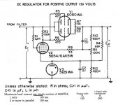
In addition, here's what I have for a modified NBS +170V regulator. It has a few things that look attractive to me.
- 3 octal tubes for 3 octal sockets
- Uses parts I already have
- Looks like it performs well enough
I have a 500VCT 150mA power transformer that should work for this. I'm thinking I could use the center tap, use UF4007 diodes. Put a choke input filter on the B+ side, which should give me about 225V (250V*0.9). Then I could use another two UF4007 diodes to make a negative supply off the same windings. Then use a cascade of RC filters to bring the negative voltage down from -350V (250*1.4) to -225V, which would charge the 0D3.
The downside is a bit of complexity.
Attachments
Last edited:
here's some-old
page 67, 150 volt regulated ps using 520 vct pt
http://www.americanradiohistory.com/Archive-Poptronics/50s/59/Pop-1959-09.pdf
page 28
http://www.americanradiohistory.com/Archive-Audio/60s/Audio-1961-Jan.pdf
( next-not 150 volts, but other voltages)
page 52
http://www.americanradiohistory.com/Archive-Service-Magazine/50s/Service-1957-09.pdf
Last edited:
Tried it. It looks like its ripple rejection would be about -40dB, since you can't put a large value capacitor in parallel with the 0D3, which is on the DC output. A C-R-C filter in front of it would make things work.
My only complaint is that M1, the upper MOSFET in the cascode CCS, will dissipate 5W and so will need some kind of heatsink. Minor problem. I have some screw-on, freestanding heatsinks, sort of like the clip-on ones but larger, meant to stand up in free air (not affixed to the chassis). I think that would be okay for dissipating 5W.
I like this Aavid-Thermalloy Part: 529902B02500G - Aavid quotes thermal resistance on their parts, which is quite useful when calculating whether or not the heat sink will be effective enough.
Also, I worry that the 0D3 would pass too much current at turn-on. With 10mA drawn by the load, the 0D3 would be passing 53mA (max is 40mA). At the target 55mA load, the 0D3 would draw 8mA. Is going that far over the max current momentarily at turn-on likely to fry the 0D3?
OD3 is quoted as tolerating 100mA on start-up for 10 sec. max on the Sylvania specs sheet.
I can see why Morgan Jones used zener diodes instead in his "Statistical Regulator." A string of 5W zeners (or even 1W zeners) won't get overloaded at turn-on. You can also put a larger cap on the output (10uF or so) and get much better ripple rejection. But again, they don't glow.
The statistical regulator works just as MJ describes, but it is tedious to solder all those zener diodes.
Last edited:
I like this Aavid-Thermalloy Part: 529902B02500G - Aavid quotes thermal resistance on their parts, which is quite useful when calculating whether or not the heat sink will be effective enough.
I have a couple of salvaged heatsinks that look a lot like that. If the TO220 part I have is dissipating 5 watts, that should be plenty. I'd need to use one CCS-OD3 per channel.
The problem is that in simulation, this DN2540 cascode-0D3 shunt circuit offers only 34.5dB ripple reduction, as compared to >60dB from the series regulator circuits. I think the only way to get this to work well would be to use zener diodes instead of the VR tube, so that you can use a larger value cap on the output (like 10uF to 20uF), instead of the 0.1uF max stated in the 0D3 data sheet. Increasing that to 0.47uF doesn't improve it enough. So in other words, make a Statistical Regulator. Oh well.
OD3 is quoted as tolerating 100mA on start-up for 10 sec. max on the Sylvania specs sheet.
Thanks. I missed that but now I see it.
The statistical regulator works just as MJ describes, but it is tedious to solder all those zener diodes.
I have a friend who has wired up a couple of them. He made a quick PCB to make it easier. He says it performs well and made his phono preamp sound better than with a Maida regulator, FWIW.
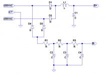
I modeled a plain old LRCRC psu using the aforementioned 10H 141R choke,
100uF after the choke, and two RC sections of 220R and 800uF 330V. PSUD2 reports a minuscule 56uV ripple at the psu output. LTspice reports ripple reduction of 46.5dB, which is not too shabby. No glowing parts
, but since I can afford to drop 60V at 110mA, I can get away with passive here. I've spent a little time today deciding on a layout and drilling holes. I'm going to try to get this thing working with a simple passive supply, then see if I can stuff the parts necessary for the NBS 150V regulator in there.
--
Last edited:
here's some-old
page 67, 150 volt regulated ps using 520 vct pt
http://www.americanradiohistory.com/Archive-Poptronics/50s/59/Pop-1959-09.pdf
page 28
http://www.americanradiohistory.com/Archive-Audio/60s/Audio-1961-Jan.pdf
( next-not 150 volts, but other voltages)
page 52
http://www.americanradiohistory.com/Archive-Service-Magazine/50s/Service-1957-09.pdf
Good stuff! Thanks for this.
Rather than the statistical regulator approach, I was suggesting you keep the pass device, but feed the VR with a CCS. I thought the low ripple rejection you modeled could have been a result of the ballast/VR AC divider. See below.

Haven't tried this, but since you're modeling I thought it would be an interesting this to try. Based on the direction of the discussion I wasn't sure if I communicated clearly what I was thinking.
Feed the above with whatever filter you like, of course. I just had this simplified schematic already worked up from a past discussion/project.
^ I've done that before and it works great. If you want a soft start feature you can add an RC filter in series with the gate resistor, with a largish resistor and a moderately sized film cap to ground you can play with parts values to get a nice ramp up feature that gives the VR tube time to settle.
OK, more fun with this! I like that idea. Perhaps I'd make two of these, one for each channel (each drawing about 55mA). That would make for a total current draw of 124mA (7mA for each of the two 0D3s, 55mA for each of the tubes). Two 0D3s on top would look lovely.
On the other hand, I was thinking I could use a couple of 6W4GT damper diodes in two of the octal sockets, feeding a choke input filter to get a calculated +208V DC. Then use plain old RC filters to get the voltage down to about +150V. Ripple would be wiped out completely, but would it sound worse than the IRF820/0D3 stabilizer?
Looks like I'm in the throes of analysis paralysis, but at least I've been collecting parts, working on a layout and drilling holes.
--
Edit to add question:
- Can I add a cap in shunt to the 150V output, after the source follower? Or will that zap the 0D3?
Last edited:
After the mosfet is fine, just don't go too crazy, I routinely put 10-47uF on the output of mine, supplying anywhere from 175-320 volts, and haven't had an issue. For low current draw this sounds like a good place to put a low ESR electrolytic or a nice leftover film cap. I've got a bunch of odd value film caps from 4-9uF that I would be inclined to put there, or even have them locally at the circuit being fed.
- Status
- This old topic is closed. If you want to reopen this topic, contact a moderator using the "Report Post" button.
- Home
- Amplifiers
- Tubes / Valves
- +150V DC Vacuum Tube Regulated Power Supply?