")
Zeners, aging, signatures?
??? Zeners have an engineered-to-be-sharp reverse breakdown which does not “age” in a well-designed use-case. But even if the case isn't “well-designed” (i.e. is subject to large over-currents, spikes, etc., where the reverse-breakdown diode is driven deep into power dissipation), the obvious solution (as with all things “power supply”) is capacitive filtering of the little devil.
FETs (MOSFETS in LinWelli's case) in a power supply are serving the purpose of sharply regulating the incoming (drain side) unregulated, “bumpy” DC relative to a voltage reference on the gate to a far smoother regulated version on the source pin. The power supply may itself therefore have a “sonic signature”, but it is a function of having a well-regulated, kilovolt-per-second source-follower in the thing, not because it is a MOSFET per se.
Seriously though… I and Lingwell agree on this one: the best solution is regulation relative to a voltage reference. Whether it is a ZENER-provided voltage reference or a pair of convenient resistors in series to make a voltage divider (either design with a suitable smoothing capacitor), is the key. Or you could use gas discharge tubes. They're pretty in service as they glow nicely. The advantage of a hard “physics” reference (like GDTs or Zeners) is that they're operating point is independent of mains voltage, or surges, or fluctuations of most-any type.
Anyway.
Just had to add my 2¢.
Sorry if it offends anyone.
GoatGuy
No reason to use zeners, just set the gate voltage with a resistor divider a couple volts above the desired voltage (to make up for the several volt drop gate-source) and run a capacitor from this junction (10uF is plenty) to ground. A standard zener from gate-source just for protection is customary, but some may say unnecessary. This will give a pretty damn stable, very quiet supply for like 3-4$USD, and a scrap heatsink. Like Goat says, you can run a reference voltage from zeners or VR tubes, but a few volts mains variation wont hurt, especially if you are in the habit of running things under max dissipation for longevity. Use a pot as the upper resistor in your divider to make things adjustable.
I wouldn't worry about "absolute" voltage regulation for much more than very sensitive circuits, or pentode/tetrode screen supplies. Case in point- my current amplifier PSU design is for a push-pull 6P43P-E design, I'm running one fet with a 22k/470k reference to give approximately 285 volts out for the preamp/phase splitter design, where absolute voltage within 10-20% isn't terribly important, so long as it's quiet. I'm running a string of 4x50 volt zeners off of this as reference for a second fet, with a potentiometer for adjustment of voltage for the 6P43P-E screen voltage, since it wants 150-185v in this application. The plate voltage for the outputs comes directly off of the bridge rectifier with a 330uF reservoir cap. Two fets, a handful of resistors, zeners, and caps, and a small bit of aluminum scrap for heatsink. Maybe $10USD total for three voltages, two of which will be absolutely dead silent, one of which will also be rock solid... Easy peasy, cheap and cheerful. Takes up less space than a single choke.
I wouldn't worry about "absolute" voltage regulation for much more than very sensitive circuits, or pentode/tetrode screen supplies. Case in point- my current amplifier PSU design is for a push-pull 6P43P-E design, I'm running one fet with a 22k/470k reference to give approximately 285 volts out for the preamp/phase splitter design, where absolute voltage within 10-20% isn't terribly important, so long as it's quiet. I'm running a string of 4x50 volt zeners off of this as reference for a second fet, with a potentiometer for adjustment of voltage for the 6P43P-E screen voltage, since it wants 150-185v in this application. The plate voltage for the outputs comes directly off of the bridge rectifier with a 330uF reservoir cap. Two fets, a handful of resistors, zeners, and caps, and a small bit of aluminum scrap for heatsink. Maybe $10USD total for three voltages, two of which will be absolutely dead silent, one of which will also be rock solid... Easy peasy, cheap and cheerful. Takes up less space than a single choke.
I tried one solution before...First one (with zeners) worked until something "fried" maybe the mosfet and worked no more. The last one you mention it's interesting but I havent' tried yet. I read around from some italian forumers speaking well about the use of transistorized LR8N3 regulator, that can be also improved with soft start and protection against over-current. I think it could be a valid alternative.
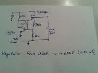
Wow… I wouldn't have guessed that circuit! But hey… whatever floats the boat, so they say. I'm guessing you have the 2n5551 in there as a kind of error amplifier? No, doesn't seem to be.
All I can tell is that Ic on 2n5551 is about 0.38 ma, as is the base current to the same transistor; Why, evades me. Sorry…
GoatGuy
All I can tell is that Ic on 2n5551 is about 0.38 ma, as is the base current to the same transistor; Why, evades me. Sorry…
GoatGuy
Wow… I wouldn't have guessed that circuit! But hey… whatever floats the boat, so they say. I'm guessing you have the 2n5551 in there as a kind of error amplifier? No, doesn't seem to be.
All I can tell is that Ic on 2n5551 is about 0.38 ma, as is the base current to the same transistor; Why, evades me. Sorry…
GoatGuy
Good morning.
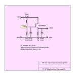
Yes, the 2N5551 should work as an error amplifier that regulates then the voltage on mosfet, through D1 and R1/R2. The reference was taken here, the second circuit:
Alimentatore stabillizzato per apparecchi valvolari
I added a little cap for a kind of soft-start, anyway it seems to work fine. As so far I didn't tested the sound because I have to complete the amp.
.... image ....
Yep. Did the math. 330 kΩ and 20 kΩ don't seem to come to 180, more like 155 following the formula. (Ironically, this is exactly what got me scratching my head wondering “how does that fly?”) The clamped-gate error amplifier design is elegantly simple. Somewhat unfortunately, adding the capacitor (for "slow start") has the unintended consequence of increasing pass-thru ripple.
It is -- at least to me -- somewhat amazing how much Italian I can understand in electronics once just a few concepts make it past the Italian→English brain barrier. Nice article. Thanks.
One last thought: if this circuit is to power up an amplifier that consumes current in response to signal substantially, you probably want to increase the capacitance of the output reservoir capacitor. I generally use 100+ μF, and if space isn't critical, 220 μF.
GoatGuy
Yes, I noticed me too this odd thing....I found empirically with that R1/R2 ratio I have 180 V output, not 155 as in theory. I have to understand why...
Anyway, I agree is a nice article explained simple.
As for the Cs I think I will not use it, rather I'll make some space for a higher output capacitor as you suggest.
Anyway, I agree is a nice article explained simple.
As for the Cs I think I will not use it, rather I'll make some space for a higher output capacitor as you suggest.
I have 2 suspicions as to why.
(1) R1 or R2 variance - simply, the “330 kΩ” or “20 kΩ” resistors are not actually those values. Could be.
(2) R3 (B+ to gate resistor) isn't 470 kΩ … same line of thinking.
I would be significantly interested to have you actually measure 4 voltages: VB+, VGATE, VSOURCE and VBASE of the 2n5551. 3 digits, please. I'm “good with the math”, so from there I can figure out what the heck the disparity is.
Yours, GoatGuy
indaco - maybe I “got it”!
Your output voltage (+180 V) is exceeding the 2N5551 maximum VCEO rating by a fair amount. (http://www.onsemi.com/pub/Collateral/2N5550-D.PDF). Turns out to be around 160 V. I know for certain that NPN junctions will become “Zeners” at the breakdown point above their rating.
So… that explains most everything, actually.
Probably want a different transistor.
2n5517, 2n6517 … both have 350 volt VCEO max ratings.
GoatGuy
Well, I made a first measurement with Vb+ = 204 V (I redid the circuit but more compact and changed a R to RC filter at input), but after discharging capacitors I obtained then a constant output voltage of 163.38 V for Vg, and Vb+ has identical value. Vs (input voltage) is always 375,15 V. Vb for the transistor is 8,641 V.
...Ic on 2n5551 is about 0.38 ma, as is the base current to the same transistor; Why, evades me....
It is the dead-classic regulator, going back to pentodes and gas-tubes.
The divider current is indeed similar to emitter current. That would be generous for an audio amplifier, but a DC Power regulator can usually spare the current.
The Base current is of course not the emitter current but 1/hFE of that.
And these values make sense. The base impedance of the transistor may be around 30K. The 18.86K divider impedance is hardly "low" compared to this, which may be part of the 180V/150V discrepancy.
Attachments
Yep. The lower-left transistor acts as an error amplifier as well as an output-to-reference comparator.It is the dead-classic regulator, going back to pentodes and gas-tubes.
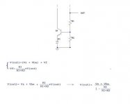
I don't think I had quibbles with the pass thru current of the v-divider. Where I had (and still have) issues is that the v-divider at 180 top-of-stack volts results in 14.4 Thévenin volts. In series with a 18.9 kΩ Thevenin equivalent resistor. And VB = VBE (0.7) + VZ (8.2) → 8.9 volts or so. So ΔV = (14.4 - 8.9 → 5.5 v).The divider current is indeed similar to emitter current. That would be generous for an audio amplifier, but a DC Power regulator can usually spare the current.
Since E = IR, I = E/R, E = 5.5 and R = 18.9 kΩ, I = 0.29 mA. If hFE = 100, then ICE should be 29 ma. It is not. It is (360 - 180) ÷ 470 = 0.38 mA. See the issue?
… what I just said, above.The Base current is of course not the emitter current but 1/hFE of that.
Pulled that one out of where? BASE “impedance” is a misnomer for BJTs in a grounded-emitter (even if thru a zener) configuration. They don't have an E/I curve that's resistive.And these values make sense. The base impedance of the transistor may be around 30°K.
Could be. There's clearly more in play than what it seems on the surface. I continue to think the transistor has been driven into VCEO breakdown, being only a 160 V rated device, bearing over 180 V. I know - from practice - that VCEO breakdown is a very zener-like sharp-corner phenomenon.The 18.86 KΩ divider impedance is hardly "low" compared to this, which may be part of the 180V/150V discrepancy.
GoatGuy
Myself, I would have used this: (attachment)
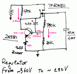
Well, I tried today this circuit but seems not regulating as expected here, also, trying with different mosfets the output voltage was slightly different. The voltage range is from 260 to 290 V. What was wrong??
Dunno. Its helpful to have both the OUTPUT voltage and the MOSFET gate voltage measurements at hand. And of course the INPUT voltage. If you implemented the whole thing, and the MOSFET(s) you used have gates which can take “the tension” (remember: I specified a particular MOSFET), then the numbers ought to be indicative.
So… what manufacturer part numbers did you use?
Keep notes, my friend. I'll keep up with the comments.
GoatGuy
So… what manufacturer part numbers did you use?
Keep notes, my friend. I'll keep up with the comments.
GoatGuy
- Home
- Amplifiers
- Tubes / Valves
- PSU for 6N13P tube