Hello!
I've been using a Bewitch 6550 (inexpensive Chinese tube amp) for a while with a few modifications (NOS tubes, improved choke & coupling capacitors, properly rated cathode resistors, etc). I am pretty happy with the way it sounds.
However, no one has been able to explain the operation of the first 2 stages of the amplifier yet. I saw a handful of posts about this on various forums, but there was no conclusive answer.
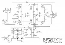
Can anyone look at the schematic (attached) and explain what is going on there? Undoubtedly one or both of the stages is performing the phase inversion, but each stage uses a different type of tube (6SL7 for the first, 6SN7 for the second). It doesn't seem like the phase inversion is completed within one stage. How and why does this work? Doesn't the push-pull signal end up lopsided going into the driver tubes? And what exactly is the top half of the 6SL7 doing with the grounded grid?
This is simply a matter of curiosity, as I have decided to rebuild the amplifier with a new circuit based on the well-known Williamson amplifier. Any answers would be greatly appreciated!
I've been using a Bewitch 6550 (inexpensive Chinese tube amp) for a while with a few modifications (NOS tubes, improved choke & coupling capacitors, properly rated cathode resistors, etc). I am pretty happy with the way it sounds.
However, no one has been able to explain the operation of the first 2 stages of the amplifier yet. I saw a handful of posts about this on various forums, but there was no conclusive answer.
Can anyone look at the schematic (attached) and explain what is going on there? Undoubtedly one or both of the stages is performing the phase inversion, but each stage uses a different type of tube (6SL7 for the first, 6SN7 for the second). It doesn't seem like the phase inversion is completed within one stage. How and why does this work? Doesn't the push-pull signal end up lopsided going into the driver tubes? And what exactly is the top half of the 6SL7 doing with the grounded grid?
This is simply a matter of curiosity, as I have decided to rebuild the amplifier with a new circuit based on the well-known Williamson amplifier. Any answers would be greatly appreciated!
Attachments
Last edited:
It's an ordinary ltp where V2 is the phase splitter.
The upper half of V1 only creates a suitable voltage to the upper V2, something
a resistor and a cap does much better.
It's also an oldfashioned ltp that does not use a current source but a simple resistive
cathode load, thus i do expect it to be unbalanced without adjustment possibilities.
The upper half of V1 only creates a suitable voltage to the upper V2, something
a resistor and a cap does much better.
It's also an oldfashioned ltp that does not use a current source but a simple resistive
cathode load, thus i do expect it to be unbalanced without adjustment possibilities.
OK. That seems to make sense. Thank you!
One question regarding the power supply. I am going to keep the power supply from this unit when I redesign the amplifier. I have changed the choke to 1.5H, 27ohms, 500mA. It looks ok in PSU Designer II, with 32mV P-P ripple. A 5H choke with nearly identical resistance and current rating provides only 9mV ripple in the simulator. Is it worthwhile to increase the inductance of the choke?
One question regarding the power supply. I am going to keep the power supply from this unit when I redesign the amplifier. I have changed the choke to 1.5H, 27ohms, 500mA. It looks ok in PSU Designer II, with 32mV P-P ripple. A 5H choke with nearly identical resistance and current rating provides only 9mV ripple in the simulator. Is it worthwhile to increase the inductance of the choke?
Well, imho there is something fishy about the LTP-circuit.
I would expect cathodes of V1 to be interconnected directly and not separated by R2 & R3.
Perhaps values for R1 (100-Ohm) and R2-R3 (2,2KOhm) got switched ?
Also the NFB through R14 should be injected into V1b's elevated grid.
Possibly elevated by around 100-Ohm.
That would possibly mean that V3/V4 anodes and screen-grids should be connected to the opposite A/G2 connections of T1.
Yes, it's a mess
Yes, it's a mess
I'm surprised it sounds so good given how odd the circuit is
As Petertub said, the LTP is V2a/b. V1a is a voltage amplifier, and NFB to the cathode is OK. V1b only provides the correct DC voltage for V2b. A quick check shows more than 10% imbalance in the LTP due to the short tail. Provides "nice" 2nd harmonic distortion in the output stage.
NFB to the cathode is OK.
Also when cathodes are separated like in this LTP ?
That's about it, but the unbalance is (more or less) compensated by R1.It's an ordinary ltp where V2 is the phase splitter.
The upper half of V1 only creates a suitable voltage to the upper V2, something
a resistor and a cap does much better.
It's also an oldfashioned ltp that does not use a current source but a simple resistive
cathode load, thus i do expect it to be unbalanced without adjustment possibilities.
A part of the input is feed via V1b to the other grid of the phasesplitter.
You could say a different solution than unequal anode resistors.
Mona
HI
This schematics was patented by a french man in the 50s : LOYEZ
V1 is the phase splitter with an important mismatch in the amplitude because the commun resistor in the cathode s very low.
This amplitude mismatch is canceled by the feedback.
R14 set the amplitude balance of the phase splitter.
Feedback rate and amplitude balance are linked.
Jacques
Last edited:
If we accept that this circuit, in AC terms, is not as daft as it looks then there is still a DC problem: the bias for V2 depends on good balance in V1.
The circuit around V1 is quite 'clever'. At first glance it looks balanced (good for marketing?). A closer look shows that V1b does little apart from setting bias for V2b (poor design). Then with the help provided by Hyperman75 an even closer look shows that V1 might be pseudo-balanced, provided that the overall forward gain and feedback fraction are carefully chosen so that V1b and V1a have similar g-k signal voltages. Assuming that the designer got this right, any change (e.g. less or more feedback, valve ageing, triode/UL switching) will knock it off balance.
The circuit around V1 is quite 'clever'. At first glance it looks balanced (good for marketing?). A closer look shows that V1b does little apart from setting bias for V2b (poor design). Then with the help provided by Hyperman75 an even closer look shows that V1 might be pseudo-balanced, provided that the overall forward gain and feedback fraction are carefully chosen so that V1b and V1a have similar g-k signal voltages. Assuming that the designer got this right, any change (e.g. less or more feedback, valve ageing, triode/UL switching) will knock it off balance.
I did a quick simulation. If R14 is chosen carefully the phase splitter is indeed balanced (theoretically....). The small signal at V1b anode cancels out the imbalance caused by the short tail in the LTP. Very inflexible design though, and as DF96 said it can be knocked off balance by many things.
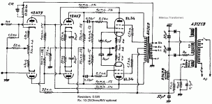
Here is the original french patend (in french)
P Loyez was not happy with the LTP phase splitter (déphaseur de Schmitt in french), because of the need of a capacitor to shunt the second grill to the electrical ground.
After long period of trials in the mid of the 50s he found the solution : an additionnal triode !
R14 is tuned to balance the phase splitter. Also 2 internal loops to help.
A Mullard 5-20 topology is much more simple and easy to understand how it works.
Jacques
Attachments
The ironic of this is that the cap that was eliminated don't carry any audio signal it's only grounding any AC !Like most attempts to get rid of capacitors, this idea (although clever) may be worse than the capacitor.
there is still a DC problem: the bias for V2 depends on good balance in V1.
I have been building a similar circuit from a DC standpoint for about 10 years. If you apply an adjustable DC offset to the (un)grounded grid of V1 the DC voltage can at the plates of V2 can be adjusted to be equal.
Set the voltages to be equal on initial power up, and fine tune for best distortion after the whole amp is operational. I usually set for minimum 3rd and higher orders, and let the 2nd fall where it may. It should only take a small tweak of the pot. If it doesn't you may have a tube with poorly matched sections.
I use a CCS in the tail of each triode pair which makes both of them true LTP's. This does require a negative voltage source capable of 5 to 20 mA depending on tube choice. I have built this with a 6SL7 or 6SN7 for V1 (depends on gain requirements) and a 6SN7 for V2. I also have a board that uses 9 pin tubes. V1 can be a 12AX7, 12AT7, 5751, 5965, 5963, 6922, 6GU7 or 6CG7 and several others. V2 is usually a 6CG7 or a 5693 (good 12AU7) or other pin compatible tubes.
If GNFB is desired it can be injected at the bypass cap on the DC offset pot (C1) via a small resistor in series with it's ground leg.
The schematic is enclosed. Mosfet drivers are included for driving just about any tube. There are resistors connected to the plates of each triode for plate to plate local feedback (often called Schade). Two series resistors are used for high voltage operation. This board has been tested to 550 volts of B+ without issues producing 200+ watts from 4D32's and 100 watts from KT88's.
Attachments
- Status
- This old topic is closed. If you want to reopen this topic, contact a moderator using the "Report Post" button.
- Home
- Amplifiers
- Tubes / Valves
- Can someone explain this confusing schematic?