Putting a CCS tail under the 2nd stage would largely fix the DC drift issue, and would automatically equalize the phase inversion. The larger signal amplitude at the 2nd stage would produce some 3rd harmonic dist. with the CCS tail though.
One would like to put a critical tail resistance (a relatively low value R) there to remove the 3rd harmonic.
I think I would go with a differential CCS tail splitter up front, then a critical tail resistance LTP for the 2nd stage, adjusted to null 3rd harmonic dist. for both stages. And then put some local output plate to LTP driver cathode N Fdbks in for local N Fdbk. (the 2nd stage LTP driver cathodes separated by two low value resistors to form the N Fdbk attenuator base, and the critical tail resistance below that).
Last edited:
But indeed it makes a big change and this is the subject of the patent !!!!....
Makes no big change in the overall circuit.
Mona
Putting a CCS tail under the 2nd stage would largely fix the DC drift issue, and would automatically equalize the phase inversion. The larger signal amplitude at the 2nd stage would produce some 3rd harmonic dist. with the CCS tail though.
One would like to put a critical tail resistance (relatively low value R) there to remove the 3rd harmonic.
I think I would go with a differential CCS tail splitter up front, then a critical tail resistance LTP for the 2nd stage, adjusted to null 3rd harmonic dist. for both stages.
Yes you can do that but it's no more a Loyez phase inverter.
And don't forget that in the 50s CCS were not easy and cheap to use.
Jacques
"And don't forget that in the 50s CCS were not easy and cheap to use."
True enough.
I wonder if one could put something like a floating paraphase correction link resistor(s) back to the input cathode resistors junction to fix any imbalance. Have to check the phasing. Maybe could come from the 2nd stage plates if necessary.
The Floating Loyez Phase Inverter:
The cathode input is in phase with the 1st stage plate outputs, so the floating correction needs to come from the 2nd stage plates. Could put a small resistor in series with the R9, R10 junction back to B+ to pick up any imbalance. Then a cap and high value resistor from the R9, R10 junction back to the R2, R3 junction. The series cap might be optional if the R_fdbk resistor value is high enough.
(but a nightmare circuit to design now, maybe OK for just fudging with a floating_feedback pot)
Hmmm, looks like it might fix the DC bias problem too.
Hmmm, another alternative would be to put the floating Fdbk from the 1st stage plate resistor junction back to the 1st stage V1b grid. (small series R from R_plates junction to B+ again for sensing imbalance)
Attachments
Last edited:
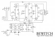
For a good laugh, you can check out the modification at Bewitch , obviously he had no clue what he was dealing with...
"Some of my modifications ideas:
1. Replace the input tubes - 6N9's with russian 6N8's or USA 6SN7GT or similar (all four octal tubes can be the same). At the cost of some amplification ratio (overall volume) we get much cleaner sound. The currents is adjusted by the resistor change in first tubes. as on the picture below.
2. Remove global feedback loop. If you find a problem - use 200K instead of 100K in the loop.
3. remove R22 and replace it with a MKP cap."
Truly idiotic...
Floating Loyez Phase Inverter:
As with the floating paraphase inverter, one can slightly unbalance the value of the sensed plate resistors to get a floating Fdbk signal that -exactly- equalizes the phase balance. (mainly useful for the version from the 1st stage plates to V1b grid. No need for the high gain N Fdbk from the 2nd stage plates then.) Not necessary to imbalance the plate R's however if the input cathode R's are already accurately nulled. (the pot in the cathodes to the tail R)
This might seem a bit redundant once the plate R's are unbalanced slightly, or the input cathode balance pot is added, but it is self adjusting versus tube aging etc.
FLPI , the "flippy" inverter?
Last edited:
The guys from Bewitch made 2 big mistakes
1 to allow to change the power stage mode : each mode has a different voltage gain so the feedback should be changed to maintain the amplitude balance
2 first stage should be with 6N8P (with lower Rp than 100 k) et second stage with 6N9P
And the guys from Lampizator understood nothing....
1 to allow to change the power stage mode : each mode has a different voltage gain so the feedback should be changed to maintain the amplitude balance
2 first stage should be with 6N8P (with lower Rp than 100 k) et second stage with 6N9P
And the guys from Lampizator understood nothing....
I see, the feedback current making the same voltage over Rc as the Vgk of V1a.Something to think about (sleep on itBut indeed it makes a big change and this is the subject of the patent !!!!
 ) but it doen't sound nice.looks like the feedback is allmost balanced out .
Mona
If one has a (global) loop gain of say 10, then about 10% (1/10) of the N Fdbk gets cancelled by the P Fdbk on the other side. Should be OK for reasonable global loop gains, not so good for low ones though.
Something like: P Fdbk = to the Input - N Fdbk for phase balance, with Input - N Fdbk = Input/(excess gain)
When one looks at the final schematic in the patent, or the one posted by jfetter, with UL Fdbks, Schade Fdbks, crossed Fdbks to the driver grids, and global N Fdbk. One has to wonder if any global excess gain was left over. Maybe just fake global N Fdbk. (the P-Fdbk cancelling the global N-Fdbk)
Last edited:
CORRECTION!
on the Floating Loyez Phase Inverter idea:
In posts 44 and 46 I made a mistake of taking the floating balancing correction N-Fdbk signal from the top junction of the plate resistors (near B+ with an added series R). This does not produce the correct balancing signal. (although maybe still an interesting one, see below). The balancing signal must come from the junction of two separate high value R resistors connected directly to the plates. Just like is done for typical Floating Paraphase Phase Inverter designs.
The previous near B+ pick-off connection picks up class B like currents from 2nd H distortions within the (individual) tubes. (disturbing the otherwise constant current flow from B+ in nominal class A operation) Called common mode distortion in class A I think, a different amplification problem. This Common Mode N-Fdbk signal could be useful for distortion correction too, but not for balancing. It would have a similar effect to putting a CCS under the stage cathodes.
The correct balancing signal pick-off from the junction of separate high value R's, does also include the common mode error signal as well (any common mode V drop appearing on the plate resistors), so it tends to fix that problem as well. So this balancing signal would also help make the Loyez operate as if it had a CCS tail. (and probably adding a cap time constant back into the response from a V isolation cap in the balancing Fdbk path)
(and thus completing all the surrounding fix-ups to the Loyez to make it act exactly like a Schmidt inverter with CCS tail in the 1st place)
Yeah, the Loyez is just a design exercise. Obtuse.
Last edited:
Speeking about mistakes, i made some (many ? ) too.But comming across an unusual circuit one learn new things.
Normally a LTP with a resistor on the cathodes is only corrected with uneaqual anode resistors.
Here i got the impression it was done with a correction signal on the normally grounded grid.Looks logical, the cathode resistor prevent a perfect signal transfer between cathodes, so why not compensate the loss with a (small) signal at the what was the grounded grid.
Well that doesn't work.The correcting signal also influence the other triode who sees a smaller cathode resistance, =more gain and both anodes get more signal.The difference doesn't disappear, only gets smaller.
Only when the correction has the same amplitude as the input signal the outputs match.But that we know allready.
Mona
) too.But comming across an unusual circuit one learn new things.Normally a LTP with a resistor on the cathodes is only corrected with uneaqual anode resistors.
Here i got the impression it was done with a correction signal on the normally grounded grid.Looks logical, the cathode resistor prevent a perfect signal transfer between cathodes, so why not compensate the loss with a (small) signal at the what was the grounded grid.
Well that doesn't work.The correcting signal also influence the other triode who sees a smaller cathode resistance, =more gain and both anodes get more signal.The difference doesn't disappear, only gets smaller.
Only when the correction has the same amplitude as the input signal the outputs match.But that we know allready.
Mona
- Status
- This old topic is closed. If you want to reopen this topic, contact a moderator using the "Report Post" button.
- Home
- Amplifiers
- Tubes / Valves
- Can someone explain this confusing schematic?