Listing 321283687491 on eBay has a quality PCB based on an older Audio Note design.
The 6V6 can be replaced by the 6L6 making it a 20 watt amplifier. This can be done by changing the OPT from 8000 to 5000 ohm and the mains transformer from 235V to 244V and the cathode resistors of the finals to (560 + 600) in parrallel. No further changes are required.
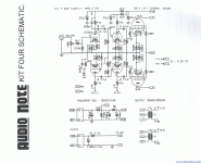
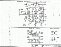
I'm attaching the AN schematics for the AN kit 4 on which this PCB is based (but much better than the AN PCB), the 6L6 schematic (it has in this later version a change of the driver tube but the 6L6 manual still mentions the same 6SN7 driver tube) and the 6L6 user manual. (PS I have seen an older schematic of the 6L6 that had the 6SN7 unfortunately I cannot find it back. I have also seen pictures of the 6L6 amplifier with the 6SN7.)
No affiliation with the seller but I was so impressed that I bought two of these PCB's.
I am building this with the tubes and transformers exposed (PCB under the top of a 2.5 inch high chassis) and hence have the capacitors and resistors on the non-labelled side of the pcb and am using a chassis from dave at landfallsystems.com who has been extreemly helpfull. (arthritis put a stop to a number of activities I can undertake, e.g making a chassis)
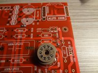
As mentioned in another post I had trouble finding some decent Octal sockets and in the end stumbled across the Omron PLE08-0 8pin sockets for inductrial use.
AM
The 6V6 can be replaced by the 6L6 making it a 20 watt amplifier. This can be done by changing the OPT from 8000 to 5000 ohm and the mains transformer from 235V to 244V and the cathode resistors of the finals to (560 + 600) in parrallel. No further changes are required.
I'm attaching the AN schematics for the AN kit 4 on which this PCB is based (but much better than the AN PCB), the 6L6 schematic (it has in this later version a change of the driver tube but the 6L6 manual still mentions the same 6SN7 driver tube) and the 6L6 user manual. (PS I have seen an older schematic of the 6L6 that had the 6SN7 unfortunately I cannot find it back. I have also seen pictures of the 6L6 amplifier with the 6SN7.)
No affiliation with the seller but I was so impressed that I bought two of these PCB's.
I am building this with the tubes and transformers exposed (PCB under the top of a 2.5 inch high chassis) and hence have the capacitors and resistors on the non-labelled side of the pcb and am using a chassis from dave at landfallsystems.com who has been extreemly helpfull. (arthritis put a stop to a number of activities I can undertake, e.g making a chassis)
As mentioned in another post I had trouble finding some decent Octal sockets and in the end stumbled across the Omron PLE08-0 8pin sockets for inductrial use.
AM
Attachments
Last edited:
My experience with this PCB is not very positive.
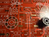
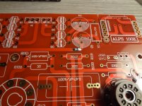
It has a serious bug that drove me crazy for quite sometime, one of the caps is shorted causing a severe oscillation; I can't understand how a defective design like this one can be commercialized without even basic testing.
Also, it has an awful lot of gain (350mV for full power), which makes it a bit noisy.
And price is not cheap either...
350mV was a very common input value 30, 40 years ago and it does not worry me. Yes it is not a cheap PCB but it is of a higher than normal quality (thicker board and thicker tracks and gold plated). However this is not a cheap design with a minimum of parts and the PCB is better than what Audio Note provided. The present design, P1-PP, is just a later development of the same except using miniature tubes that have a far shorter lifespan.
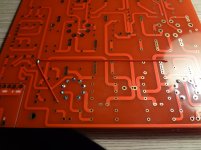
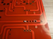
Honestly it does not surprise me that there are some problems - there are two errors in the PCB: the DC feed to the 12AX7 is shared with the signal paths so you'll have to cut two tracks and pull two wires. The second problem is that the first 33uF capacitor to follow the 220uF capacitor should have a resistor in it (check the 6L6 design) which means that you have to cut somewhere the HT track.
Was the shorted capacitor a PCB error or just a faulty part?
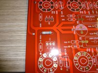
There is also a design error: the original design had bypass capacitors on the cathodes of the 12AX7 giving a gain of approx 40 and which works out pretty OK for the resistor values of the floating paraphase splitter. Later pictures show these spaces to be left empty on the PCB and the schematic also no longer shows these capacitors. By leaving these out the gain of the 12AX7 drops to approx 14 which changes the values of the resistors of the floating paraphase splitter. My calculations suggest R8 = 220K, R9 & R11 = 270K and R23 = 0. I'll use a trimpot initially to confirm these values and then will replace it with fixed resistors.
I'm attaching photo's of the changes to the PCB.
Honestly it does not surprise me that there are some problems - there are two errors in the PCB: the DC feed to the 12AX7 is shared with the signal paths so you'll have to cut two tracks and pull two wires. The second problem is that the first 33uF capacitor to follow the 220uF capacitor should have a resistor in it (check the 6L6 design) which means that you have to cut somewhere the HT track.
Was the shorted capacitor a PCB error or just a faulty part?
There is also a design error: the original design had bypass capacitors on the cathodes of the 12AX7 giving a gain of approx 40 and which works out pretty OK for the resistor values of the floating paraphase splitter. Later pictures show these spaces to be left empty on the PCB and the schematic also no longer shows these capacitors. By leaving these out the gain of the 12AX7 drops to approx 14 which changes the values of the resistors of the floating paraphase splitter. My calculations suggest R8 = 220K, R9 & R11 = 270K and R23 = 0. I'll use a trimpot initially to confirm these values and then will replace it with fixed resistors.
I'm attaching photo's of the changes to the PCB.
Attachments
Last edited:
A quality PCB doesn't have errors.
Implementations always have to deal with compromises: different implementers will often have different solutions. What I regard as an error someone else may find acceptable, expecially if we compare this with solid state implementations. I'm a bit OCD in that regard.
On a side note: the OPT's in this case are very important since we deal with three stages of amplification and phase shift plays a role. An OPT that is not up to scratch will cause unstability where a two stage setup is far more forgiving. This was something that the original Williamson amplifier builders found out: the OPT had to be constructed just in that particular way otherwise instability was the result.
Last edited:
- Status
- This old topic is closed. If you want to reopen this topic, contact a moderator using the "Report Post" button.