Ok Great....please put me down for a pair of board, what could also be very helpful would be a nice layout templet ") actually after i wrote this i thought just put small hole in the middle of each tube this will be easy as pie then i can center punch and drill
actually after i wrote this i thought just put small hole in the middle of each tube this will be easy as pie then i can center punch and drill
Lawrence
actually after i wrote this i thought just put small hole in the middle of each tube this will be easy as pie then i can center punch and drill Lawrence
Last edited:
It would be pretty easy to simply print out a copy of the PCB, then you can lay it on top of the chassis, and center punch the locations to be drilled. Easy peasy
No it’s eaiser my way

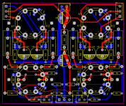
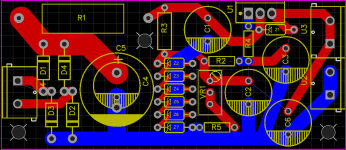
Moved some more things around a smidge, scooted the top sockets down further for better clearance between the mounting holes and the output terminals, made all the small solder pads 2mm ( ) for ease of use, moved the coupling caps down a bit for better access to the upper mounting screws, and nested a smaller resistor footprint into the filter resistor.
I'm feeling like we are getting pretty close to calling it done!
) for ease of use, moved the coupling caps down a bit for better access to the upper mounting screws, and nested a smaller resistor footprint into the filter resistor.I'm feeling like we are getting pretty close to calling it done!
Attachments
Good work! The electrolytic capacitors in the same orientation will decrease the chance of a mistake. For film capacitors, it would be useful to mark the outside foil connection on the silkscreen. Heater wiring is point to point, so it would be nice to have the provision for an additional unconnected 2-way pluggable terminal block. It would make possible to tie the heater wires on that terminal block solder pads. Less clutter inside the chassis and the filament supply will be easily disconnected from the PCB when necessity arises.
You mean like an additional 2P terminal in the corner somewhere in the corner(s), meant to daisy chain the wiring to? That could be useful, with the twisted pair just jumping from point to point on the board itself...
I had toyed with the idea of even putting terminals at each socket, but I figured they would be too bulky so decided to go P2P for the board.
I had toyed with the idea of even putting terminals at each socket, but I figured they would be too bulky so decided to go P2P for the board.
Taking a break from the amplifier board to work on the companion board, a mosfet ripple filter ("capacitance multiplier") board, with onboard rectification. A string of six zener diodes for a voltage reference, and a trimpot for fine adjustment for setting operation points a bit more precisely. Should be more versatile for use with screen supplies for larger amps, etc. You can also use a single resistor as a reference and leave out some parts to make a simple capacitance multiplier too. Current size is 32.5x75mm. I plan to make a single and a dual version.
Attachments
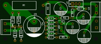
Alright, printed out a 1:1 copy of the PSU, and it looks like it would make more sense to extend it to 32.5x100mm, that way I can space out the caps better for some more options in bigger footprints for them. Should be a bit better. It's still really small!
Why 32.5x100? I can fit three of them in the 100x100 promo price from JLCPCB, and that will make them cheap as chips
Why 32.5x100? I can fit three of them in the 100x100 promo price from JLCPCB, and that will make them cheap as chips
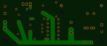
I've got holes on there, they just don't show up well on the render
For this one, the intent is to mount the mosfet to either the chassis or a small heatsink off to the side. I'm not a fan of heatsinks on board, as it limits your options. The best way to go would be an isolated tab fet, and bolting to a small heatsink or piece of aluminum angle that is bolted to the chassis. For moderate power it won't dissipate much heat, so solutions are easy
There are a few obvious errors that have already been corrected, btw. I'll mess with it more tonight.
Last edited:
Re the heatsinks, I'd agree personally. I was thinking about novices and having a foolproof build option for folks who don't know how much heatsink is enough. Agreed on the insulated tab option too. That schematic I posted a while back specifies such a part - probably a good option when you come to do a bom.
With regard to the three PCBs on one board- one of the old gb's did 2*positive andb1*negative for all buyers of that PSU design. It was suprisingly handy! This board is potentially suitable for SS preamps and such as well, so a negative rail version might be quite helpful!
A negative version had crossed my mind for sure, and would be very handy for bias supplies, dual rail supplies for source followers for driving power tubes, and even for use with solid state types of builds (gainclone and pass types of builds come to mind) that don't need absolute perfection, just quiet supplies. I'll do a negative version for sure now
Done. I'll try to figure out what else to throw in that 20x100mm area off to the side, and need to add V-cuts to separate the panels. I'm not super well versed in P-channel stuff, so I hope it looks ok, but so far I think it should all check out. Needs more looking over and polish, but it seems pretty close.
Attachments
Alright!
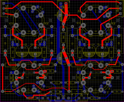
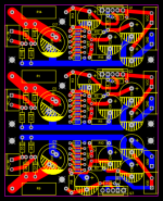
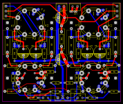
Did some last minute checks on the amplifier board. Added a 2P terminal for the heater wiring to bounce off of (which may be useful for some builders) and I think I'm happy with it. I'll still be fooling with PSU boards for at least the next few days or longer.
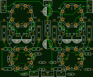
FINAL DRAFT!
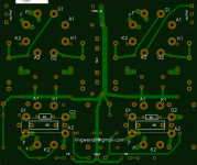
If there aren't any issues or last minute comments I'll be ordering boards tomorrow (don't worry, I'll let you guys know when I do) to check out. Don't put in your word for any boards until I have a working prototype in hand, and at that point I'll start a group buy thread for ordering info.
Did some last minute checks on the amplifier board. Added a 2P terminal for the heater wiring to bounce off of (which may be useful for some builders) and I think I'm happy with it. I'll still be fooling with PSU boards for at least the next few days or longer.
FINAL DRAFT!
If there aren't any issues or last minute comments I'll be ordering boards tomorrow (don't worry, I'll let you guys know when I do) to check out. Don't put in your word for any boards until I have a working prototype in hand, and at that point I'll start a group buy thread for ordering info.
Attachments
- Home
- Amplifiers
- Tubes / Valves
- 6SN7 push pull flea amplifier project