Hello all.
Need some help here in identifying these amplifiers.
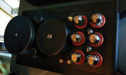
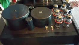
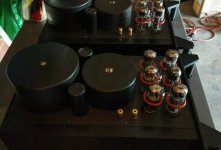
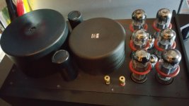
I recently purchased these from a Sydney seller and one can clearly see that they have been home built.
My gut feel is that they were made in Australia.
I would very much like to find out, if possible, who built them (so I can badger them with lots of questions!!!)
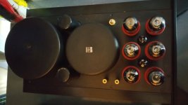
They are reasonable well made, and with each amplifier running 2 x 6NS7 and 6 x EL34.
What is interesting, is that the main circuit board holding all the tubes looks to be of commercial quality, being sully silk screened, solder masked and plate through holes. The rest is hard wired.
Transformers, both power and output are Plitrons.
If you can help, I would be very grateful to hear from you - Perhaps you recognise the casework?
PS I will post some internal pictures tonite.
Kind Regards
George.
Need some help here in identifying these amplifiers.
I recently purchased these from a Sydney seller and one can clearly see that they have been home built.
My gut feel is that they were made in Australia.
I would very much like to find out, if possible, who built them (so I can badger them with lots of questions!!!)
They are reasonable well made, and with each amplifier running 2 x 6NS7 and 6 x EL34.
What is interesting, is that the main circuit board holding all the tubes looks to be of commercial quality, being sully silk screened, solder masked and plate through holes. The rest is hard wired.
Transformers, both power and output are Plitrons.
If you can help, I would be very grateful to hear from you - Perhaps you recognise the casework?
PS I will post some internal pictures tonite.
Kind Regards
George.
Attachments
If you meant 6sn7, they're not. 6sn7 is an octal tube. Pull one out and read the printing on the tube.
Thanks for the correction.
Lets try 2 x 6CG7
Cheers.
George.
Hello again.
These amplifiers continue to be a source of frustration. Main issue is stability, and difficulties in biasing, and maintaining bias.
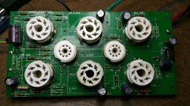
Over the past few nights, I have managed to piece together a schematic from the PCB, which was not an easy job, considering its double sided, and fully populated.
Further to my original post, herewith is a picture of the actual PCB.
Once again, I am hoping that someone recognises it, and can help me identifying the maker / designer.
The PCB is definitely of commercial grade.
If there is anyone that knows where it came from, please let me know.
Kind Regards
George
VK5ZG
PS: My sincere thanks to Ian - “Gingertube” from this site, for all the assistance he has given me to date.
These amplifiers continue to be a source of frustration. Main issue is stability, and difficulties in biasing, and maintaining bias.
Over the past few nights, I have managed to piece together a schematic from the PCB, which was not an easy job, considering its double sided, and fully populated.
Further to my original post, herewith is a picture of the actual PCB.
Once again, I am hoping that someone recognises it, and can help me identifying the maker / designer.
The PCB is definitely of commercial grade.
If there is anyone that knows where it came from, please let me know.
Kind Regards
George
VK5ZG
PS: My sincere thanks to Ian - “Gingertube” from this site, for all the assistance he has given me to date.
Attachments
The tubes are too close. The input tubes should not be in between the output tubes (HF feedback and heat). The PC traces are rather close for HV.
I don't see any trimpots for biasing the output tubes. Their appears to be an Op. Amp. chip, maybe some kind of auto-bias circuit. That still would not handle differences between the tube triplets though, unless there are some current sharing cathode resistors. Someone probably got tired of ordering matched triplet tubes. That many tubes in parallel may require some VHF parasitic absorbers (R L) in the plate circuits too.
I don't see any trimpots for biasing the output tubes. Their appears to be an Op. Amp. chip, maybe some kind of auto-bias circuit. That still would not handle differences between the tube triplets though, unless there are some current sharing cathode resistors. Someone probably got tired of ordering matched triplet tubes. That many tubes in parallel may require some VHF parasitic absorbers (R L) in the plate circuits too.
Last edited:
Hi Binary & Smoking.
I agree with both of your comments.
With respect to the PCB, whilst very well made, the layout in my opinion is quite poor, with traces literally running from one side of the board to the other just to pick up another component.
There is a separate PCB with a simple PSU for the bias supply, and this also contains the trim pots for bias adjustment.
The op amp, BB OPA2134 feeds the 6CG7 triodes at the input. Must say I have not seen this before.
I have managed to sketch out the schematic, but it still needs checking and to be properly drawn up.
I will post it as soon as I have cleaned it up
Thanks you all for your assistance.
Cheers
George.
Schematic Finally Done!!
Hello all
Proper performance for these mono-blocks still eludes me.
One of the main issues I am having is biasing is almost impossible, even with matched pairs of tubes. When you adjust one, if affects others, no matter how hard I try.
The main culprit is biasing V7 and V8, and their interaction with V6 and V5.
To move things along, I have managed to draw out the circuit diagram, which was not a pleasant task, considering what is in my opinion a very poor PCB layout, complicated by being a double sided board.
Any errors in my schematic are either my error, or an actual circuit error.
Time will tell – hopefully by more experienced valve amp members.
When I look at the schematic, It appears to me that V4 and V6 - G1 are been fed incorrectly, when you look at C8, C10, C12, The same applies for the opposing side which is a mirror image.
Ultimately I would like to strip the amps down, and re-built without the PCB I.e hard wire.
In addition to this, I can’t understand why the front end op amp is required.
I look forward to any assistance that any member can give me.
Thankyou.
Kind Regards
George.
Attachments
To mee it seems that the front-end op-amp IS the phase inverter. I do find
the schematic strange or faulty in a number of places.
Yes, if the source refuses to give a schematic, rebuild is the only way ( why did
you purchase it without proper documentation in the first place ??)
the schematic strange or faulty in a number of places.
Yes, if the source refuses to give a schematic, rebuild is the only way ( why did
you purchase it without proper documentation in the first place ??)
Hi Peter.
I purchased the amplifiers off the internet, on the promise that they were in good order, and he would suppy further documentation at a later date, once he found it.
Unfortunately once he got my money he would not respond.
I paid $800 for both amps. At the very least this is the value of all of the transformers and tubes.
I shoukd have known better.
Could you tell me where the circuit looks strange to you?
Thanks for responding
GeeVee,
Strange stuff : i'll start at the very beginning :
- The input is connected to op output, switching out and (-) input would make sense.
-it seems that only one triode is used ( or i misinterpret the lines ) on the input tubes.
-AX and BX seems to be some feedback, THROUGH electrolytic caps ??
-6 EL34 could easily be replaced with 4 6550 ( or 2 kt-150 )
- there is UL connections on the OT, but not on the tubes ...
-there is no feedback from the outside of the OT, this leaves the OT out-of-the loop
- no provision from blocking too high or too low frequencys, this can cause motorboating
at low and distorsion at high frequencys.
-no DC protection on the input
- DC B+ has only one CAP, none after the choke
- No current limiter or fuse on the mains input
etc
My advice :
Keep the chassies, junk the board and build a MkIII with 4 6550
Looks to me that the Op Amps are intended to do the phase splitting. Something drawn or connected wrong with the Op Amp output connected back to the signal input.
The 6FQ7 tubes appear to be wired up as Mu followers. The sections are in series.
AX, BX and CX I think are just signal grounds. (I don't see the ground connection made on the schematic for BX however.)
The biasing pots for the EL34s are just in series with the bias supply to the grids. There needs to be a resistor from the grid end of each of the pots to ground (AX,BX or CX?) to perform a voltage divider function. Maybe these resistors are missing on the board. Some un-populated sites on the board?
It could also use a high value resistor across each of the pots as a safety backup, in case a pot wiper opens.
Once the biasing pots are functional, should be OK with the 6 x EL34. The tubes are connected up as triodes, so the UL taps are not needed.
Power supply could use an extra cap after the inductor. Drawing error or missing part again? It could work without the cap I guess, if the Amp is biased into class A operation.
With all the input Op Amps you would think they could have provided some global feedback port, but maybe the triode outputs were being left to themselves for output Z and linearity.
There is probably some hope for getting it to work. Just not so "tube" friendly with Op Amps. Maybe could put a CCS tail under the Mu followers to perform the phase splitting instead. (in place of R5)
Yeah, a power fuse and On/Off switch would be nice. UL... approved?
Last edited:
The bias pots need different wiring than shown. The pot wiper arm should go to the 100K grid bias resistor of each tube. The pot ends should be between the -Vbias and ground. Then an additional high value safety R from each pot wiper to -Vbias added. Since this area is shown with dotted line connections, I'm guessing these connections are made with external wiring from the power supply board. Someone may have messed up the discrete wiring when it was built. Really should have all this configured on the PC board for fool-proof construction.
Last edited:
My gut feeling is that this is a diy project using some very nice components on perhaps chinese (?) boards.
I agree that Petertub's suggestion I post #12. Go with a solid design using UL Pentode and nfb to get the most out of those Plitrons. You won't regret it.
Its a pity to waste those plitrons on such a flawed build...
Ian
I agree that Petertub's suggestion I post #12. Go with a solid design using UL Pentode and nfb to get the most out of those Plitrons. You won't regret it.
Its a pity to waste those plitrons on such a flawed build...
Ian
Last edited:
Thanks
Hi all
Thanks to all of you that have replied, and made suggestions.
I made one last attempt over the weekend to try and bias them, and keep them stable, but to no avail.
What is even more interesting now, is that the other PCB is slightly different to the one that I traced out.
I'm not even going to waste my time in redrawing it.
I have decided to scrap these amps, and build brand new ones, using the Plitron OPT's and Power transformers, using 4 x KT88 or 4 x EL34 per side.
I will start a new thread shortly, once I settle on a schematic and start procuring the parts.
At least I already have the most expensive bits!!
Cheers
George
Hello all
Proper performance for these mono-blocks still eludes me.
One of the main issues I am having is biasing is almost impossible, even with matched pairs of tubes. When you adjust one, if affects others, no matter how hard I try.
The main culprit is biasing V7 and V8, and their interaction with V6 and V5.
To move things along, I have managed to draw out the circuit diagram, which was not a pleasant task, considering what is in my opinion a very poor PCB layout, complicated by being a double sided board.
Any errors in my schematic are either my error, or an actual circuit error.
Time will tell – hopefully by more experienced valve amp members.
When I look at the schematic, It appears to me that V4 and V6 - G1 are been fed incorrectly, when you look at C8, C10, C12, The same applies for the opposing side which is a mirror image.
Ultimately I would like to strip the amps down, and re-built without the PCB I.e hard wire.
In addition to this, I can’t understand why the front end op amp is required.
I look forward to any assistance that any member can give me.
Thankyou.
Kind Regards
George.
your schematic looks crazy! I would remove the 100uf caps as those should have been bypassing the cathode resistor in the circuit schematic you drew, they look like positive feedback circuit albeit not too much, but it is positive feedback.
I think I remembered seeing that board before. I think it was plitron's stab at diy kitting about a decade or so ago. the capacitors are incorrect.
when the ic dies, replace it with a input transformer. as that ic and the ones like them are no loner available in PDIP package they are all only available as surface mount now.
Until I looked at the schematic, I was unwilling to comment.
I see a big "no/no" in the setup. If the bias supply is regulated (as is the case here) the B+ supply must be regulated too.
The "iron" is good. Therefore, I suggest straight forward Williamson style circuitry, using the 6FQ7s in the small signal positions. Buffering the differential amplifier plates with DC coupled MOSFETs seems to be in order. While quite capable, the triodes in a 6FQ7 might easily be overtaxed driving 3X "fixed" bias UL mode EL34s each. Remember that EL34 grid to ground resistance limit is comparatively small, when "fixed" bias is employed, and UL mode introduces a fair amount of CMiller. An IRFBC20 source follower will "loaf" working into that potentially problematic load. Don't forget a 15 V. Zener diode between the gate and source, to protect against power on mishaps.
FWIW, I'd bridge rectify the bias winding with 4X Schottky diodes and CRC filter the rail. Eliminating PN diode switching noise in the B+ rail is (IMO) also a good idea. Constructing the B+ bridge from 4X Cree C3D03060F SiC Schottkys will do exactly that.
Hi Eli D
Thanks for your reply
I have looked at my trace of the circuit, just to make sure that I did not draw it incorrectly.
Unfortunately this was not the case, and has given even more weight to the argument as to how these amps ever worked in the first place.
I have started to strip them down, and reuse all of the transformers etc into a brand new build.
Still deciding on which circuit to build, but more that likely 4 x EL34 per side, simply because I have a lot of these tubes.
The transformers at hand are:
2 x Plitron OPT Model 4006-01 (100W)
2x Plitron Power Model 754709-02 Outputs: 340.0VAC @ 0.7A, 6.3VAC @ 6.8A, 40.0VAC @ 0.1A
2 x Chokes Hammond 1.5H, 500ma
2 x Generic 6.3 and 12.6 heater transformers.
As this is probably the most expensive parts - makes sense to re use.
Cheers
George.
- Status
- This old topic is closed. If you want to reopen this topic, contact a moderator using the "Report Post" button.
- Home
- Amplifiers
- Tubes / Valves
- Who Made These Amps.