Circuit is looking good. As has been mentioned earlier, keep the gate stopper resistors close to the MOSFET as you have drawn the schematic.
My recommendation is to have the zener protection diodes connected directly between the source and gate terminals. Move the anode of the zener diode to the junction between the gate of the MOSFET and the gate stopper resistor.
Reason is if you are probing around in the circuit while energized and connect your meter lead to the gate of the MOSFET the lead capacitance is enough to create a voltage spike across the gate stopper resistor that can blow the gate of the MOSFET.
The reason I mention this is I've blown up a few CCS's before realizing this detail. The higher the operating voltage the better the chance of letting out some of the magic smoke in the MOSFET if the protection zener is configured as shown in your latest drawing.
My recommendation is to have the zener protection diodes connected directly between the source and gate terminals. Move the anode of the zener diode to the junction between the gate of the MOSFET and the gate stopper resistor.
Reverse leakage current for these Onsemi zenners seem to be too small to affect MOSFETs, so its OK.
For testing purpose I would recommend to build separate pads with hole D ~ 1 - 1.2 mm. It's much convenient then touching component's leads, and prevents probe slipping.
Hi, sulcorebutia,
1) Do you plan to include multi-turn trim pot on the CSS add-on board?
2) What is approximate date of final product shipping?
1) Yes
2) No nothing confirmed yet.
Do you happen to know any free software that make/draw PCB layout? If I don't provide the PCB layout, the producer will use his own way to make the PCB and possibly will also ignore our concern like, heat dissipation pad or shortest distance between stopping resistor and mosfet etc.
Circuit is looking good. As has been mentioned earlier, keep the gate stopper resistors close to the MOSFET as you have drawn the schematic.
My recommendation is to have the zener protection diodes connected directly between the source and gate terminals. Move the anode of the zener diode to the junction between the gate of the MOSFET and the gate stopper resistor.
Reason is if you are probing around in the circuit while energized and connect your meter lead to the gate of the MOSFET the lead capacitance is enough to create a voltage spike across the gate stopper resistor that can blow the gate of the MOSFET.
The reason I mention this is I've blown up a few CCS's before realizing this detail. The higher the operating voltage the better the chance of letting out some of the magic smoke in the MOSFET if the protection zener is configured as shown in your latest drawing.
Gary, thanks for your input. Your experience is extremely vital to this project!!
Do you happen to know any free software that make/draw PCB layout? If I don't provide the PCB layout, the producer will use his own way to make the PCB and possibly will also ignore our concern like, heat dissipation pad or shortest distance between stopping resistor and mosfet etc.
For the beginning, you can use Eagle Freeware Edition
https://www.cadsoftusa.com/download-eagle/freeware/
Board size will be limited to 100 x 80 mm (4 x 3.2 inches), and 2 layers, that's enough for this project.
You may also try freeware open source KiCAD which is much more powerful then free version of Eagle, but I don't know how mature it is.
KiCad EDA Software Suite - Kicad EDA - KiCad EDA
Thanks LinuksGuru, I have been trying the eagle freeware edition for a whole week. With sincere apology, I couldn't get to it to work. I know it sounds too demanding, but would anybody kind enough to make a PCB layout file with this circuit? This would be huge benefit in order to get a freelance producer to accept our order. Thank you to anyone who could help.
Thanks LinuksGuru, I have been trying the eagle freeware edition for a whole week. With sincere apology, I couldn't get to it to work. I know it sounds too demanding, but would anybody kind enough to make a PCB layout file with this circuit? This would be huge benefit in order to get a freelance producer to accept our order. Thank you to anyone who could help.
Nope, its not demanding, collective effort requires collective contributions. I can design PCB, no problem. Sulcorebutia, you need gerbers and NC drill files, right? In all PCBs I made I used only through hole parts, not SMDs, but I think its not a problem to switch to SMDs. What is the footprint of multi-turn potentiometer you are going to use?
I checked again thread. BSP139 have very low power dissipation, and such CSS will have too limited application. We should use Supertex DN2540, or IXYS IXTP08N50D2 (500V, 60W) / IXTP08N100D2 (1000V, 60W) in TO220 case, which can be easily installed on heatsink. My idea is that Sulcorebutia could built and ship partially assembled CSS modules without MOSFETs, heatsink, and may be even potentiometer, then DIYers will solder any parts they want.
CSS should have 3 hole output with 5mm clearance between each, it can be fit with wires or 3-way screw terminal block like Phoenix Cpmbicon MKDS 3/3 or similar. 2nd variant is for someone who wishes to use CSS with output tubes, high current, and large heatsink.
MOSFETs can serve as mounting plates of the CSS board on heatsink. In turn, heatsink will be screwed on amplifier PCB.
Any other ideas or suggestions are greatly appreciated !
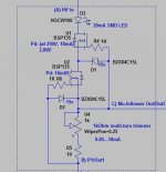
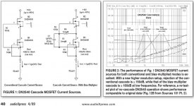
Cascoded CSS with BIAS multiplier
There is an article in AudioXpess 4/2009, which describes improved version of cascoded CSS with BIAS multiplier. Please see schematic and graphs attached.
PS. Sulcorebutia, you can omit 1uF film cap in your builds.
There is an article in AudioXpess 4/2009, which describes improved version of cascoded CSS with BIAS multiplier. Please see schematic and graphs attached.
PS. Sulcorebutia, you can omit 1uF film cap in your builds.
Attachments
Quick update for everyone interested in this:
I have been discussing with three freelance producers without any solid result.
First guy simply rejects, saying he is too busy these days.
Second guy says that he is puzzled by this circuit, even though it is much simpler than his $3USD Cree XML-U2 driver module. More importantly, he said he has no 250V power supply to test it.
Third guy is producing high wattage LED ccs and solar panel inverter for a living. So, he shouldn't be too scarce about high voltage device. But the minimum order is 300 pcs.
Frankly, it is a bit risky to make 300pcs of low cost CCS all at once. In the worst scenario there might be only 100 pcs sold successfully. And then the leftover would cost me $800USD
So, I am considering to order the PCBs first and purchase some parts from Mouser. By then I should able to build several sets to test the audio quality in real world.
Would anybody wants to receive a pair of sample to test?
Only if the test result are positive, I would dare to make 300pc order
Last edited:
Nope, its not demanding, collective effort requires collective contributions. I can design PCB, no problem. Sulcorebutia, you need gerbers and NC drill files, right? In all PCBs I made I used only through hole parts, not SMDs, but I think its not a problem to switch to SMDs. What is the footprint of multi-turn potentiometer you are going to use?
I checked again thread. BSP139 have very low power dissipation, and such CSS will have too limited application. We should use Supertex DN2540, or IXYS IXTP08N50D2 (500V, 60W) / IXTP08N100D2 (1000V, 60W) in TO220 case, which can be easily installed on heatsink. My idea is that Sulcorebutia could built and ship partially assembled CSS modules without MOSFETs, heatsink, and may be even potentiometer, then DIYers will solder any parts they want.
CSS should have 3 hole output with 5mm clearance between each, it can be fit with wires or 3-way screw terminal block like Phoenix Cpmbicon MKDS 3/3 or similar. 2nd variant is for someone who wishes to use CSS with output tubes, high current, and large heatsink.
MOSFETs can serve as mounting plates of the CSS board on heatsink. In turn, heatsink will be screwed on amplifier PCB.
Any other ideas or suggestions are greatly appreciated !
Linuksguru, thanks for your kind help. How about this? a PCB with two cascode BSP135, but "upgrade-able"?
Your idea is great, it is good to have a more robust CCS. However, we don;t need two high power DN2540/IXTP01N100D cascoded together. Only the top one is required to do the hard work and got heatsinked.
Considering BSP135 is the cheapest high voltage depletion mosfet available, if we can have a basic board of BSP135 cascode, and reserve pins out for n-channel depletion mosfet(to-220 package), then whoever wants to upgrade it can de-solder the top bsp135 and install a DN2540/IXTP01N100D/IXCP10M45S/IXCP10M90S with a suitable heat sink.
Ideally the TO-220 mosfet, which is connected to top bsp135 pin to pin, should be located at the side of the PCB.
What do you think?

Last edited:
I will SPICE CSS with BIAS multiplier at high current (e.g. 70mA), and see what is power dissipation of each mosfet. I think in this connection power is distributed among 2 transistors. Cost savings of 1 power mosfet is not something I'm concerned about.
Using BSP135 will not result in small module. According to data sheet, BSP135 needs 6 cm^2 copper area for drain connection/heat dissipation, that's 2.45x2.45 cm area.
From the BSP135 data sheet - "Device on 40 mm x 40 mm x 1.5 mm epoxy PCB FR4 with 6 cm2 (single layer, 70 μm thick) copper area for drain connection. PCB is vertical in still air."
To the op: is it possible to rename this thread to something like "CSS Kits for Tube Circuits - Ideas, Schematics & PCBs"?
Last edited:
I have two suggestions...
1. If the BSP135 doesn't work well as CCS at low current, (I don't know if that is the case), a variant (overlapped footprint?) where the lower device can be changed to a LM334?
2. Add some jumpers (zero ohm resistors) so we can easily modify the board to become a source follower with a CCS as the source resistor.
Regards,
ym
- Status
- This old topic is closed. If you want to reopen this topic, contact a moderator using the "Report Post" button.
- Home
- Amplifiers
- Tubes / Valves
- Will anybody interest in stamp size ccs module?