I will try to measure time lag in ultra linear mode ( no global feedback ) . I suspect I am in for a surprise and it will be remarkably good . I should have said about shunt feedback for input pentodes that g2 is always there and pentode distortion is always there . However I feel up to the point where full triode operation is required simple shunt feedback will do fine . One thing I must try is coupling EF184 g2 to the cathode of the next stage . Being that output EL 36 needs 52 V of cathode bias I'm half way there . Doubtless it will oscillate . It will be fun to find out . I can then use some feedback from the anode also of the EL 36 to see what happens ( via the previous stage coupling capacitor , EF 184 rp shouldn't be a problem ) . I am tempted to use a bipolar transistor for comparison as input pentode ( no cathode feedback unless a cascode ) . TIP 150 for example with clip on heat sink . I suppose a transistor inverter to drive EF 184 g2 from the output valve anode might be interesting . We are a long way from triode to pentode in stages for EF 86 pentode . I hope someone has a view on shunt feedback and EF86 . I will try a transistor UL feedback cascode . The dreaded TIP 150 again , at 10 MHz they are painfully slow so should misbehave splendidly . My only UL transformer is for EL 34 . Returning to this hypothetical amp if using shunt input stage feedback then all of the feedback mechanisms meet at one point . That seems very wrong or more likely very right .
Its interesting,
To listen to all grids to triode "true triode" as opposed to Psudo triode.
There is a difference..")
Just for fun link:
http://www.decware.com/paper16.htm
Regards
M. Gregg
To listen to all grids to triode "true triode" as opposed to Psudo triode.
There is a difference..
Just for fun link:
http://www.decware.com/paper16.htm
Regards
M. Gregg
Last edited:
"the pentode is just a high Mu triode"
-----------
"No, not really. The pentode is more like a triode in which the functions of majority current collection (anode) and voltage feedback (g2) have been separated. You don't get low distortion by giving a pentode an infinite anode load, as the distortion is set by the grid-cathode behaviour. Remember, pentode curves go the opposite way - increasing mu will not make a triode curve like a pentode."
------------
Well, the UL Mu formula: Mu_eff = gm1/(UL% x gm2 + 1/rp) doesn't take into account the screen current lost when the plate is operating near the screen voltage. If one takes the screen current and sums it back into the plate current, the "plate" curves curve upward again like high Mu triodes, in the useable region. UL partially does this via the OT tap. A Mosfet follower screen driver could sum the screen current back into the plate (via a drain to plate connection) if the plate V stays above the screen V. Fun to try on the curve tracer anyway if you can get it stable.

I went to " Chicago Mike's Rock and Roll tour of London " yesterday , strongly recommended . Was dreading getting back and probably finding no new entries . Glad to say not the case .
M Gregg . I especailly appreciate the love of EL 84 in Decware link . I think EL 156 also has the desirable separate g3 if I am not mistaken ( EL 34 has , EL 84 not ) ? I will make a list of all nice / cheap pentodes when time permits where g3 is separate . Someone I am sure has already done that ? I always said EL 84 was the best transistor ever made if you will forgive . One day I will use one as VAS in a transistor amp . An op amp will drive EL 84 ( don't put a global feedback loop on as your first experiment , if NE 5534 keep gain above 10 ) . The grid bias easy to set up on the op amp if you like to get an extra watt or so . Use inverting op amp design if practical .
Smoking Amp . I very much appreciate the picture of the current division between anode and g2 and love reference to the anode being a collector ( pentodes must be a transition resistance devices also , triodes also except they hide it ) . As is often the case most of what I try to do is like getting water to run up hill . I then need a pump . I always loved bootstrapping because then water does run uphill ( almost ) .
I might pull apart a small mains transformer and reconfigure the E's and I's ( lamination's ) to work with an air gap . It might yield some 1 kHz information about a UL transformer . If it is better than expected it might be worth trying harder . The valve under test EF 184 at 10 mA .
The circuit I draw here is what my mind said would be similar to UL feedback when this started . I use a transistor as it seems it would work without any special requirements . A MOSFET if being strict is better on bandwidth and slightly less good in linearity as this is a current amp . I doubt it would be critical for an early test either way . I doubt that anything in the true UL sense is available here ? However something better than g3 shunt feedback might be ? I am happy to be shot down in flames as no pain no gain in these things . There is no hum filtering arrangement on the g2 which is intentional . Use >1 K as the base input stopper . TIP 150 will dissipate 2 W and MJE 340 1 to 1.5 W in free air . A small heatsink will help . 10 MHz is not too bad as no voltage gain required , 30 MHz for MJE 340 .
Using the drain of a HEXFET ? That would need phase inversion ? Maybe I've missed the point and we need antiphase at g2 ? . If a HEX FET gate was connected to the EF 184 cathode the drain would be in phase with the anode . However it would represent the sum of the currents passing ( anode + g2 ) . Also it would have the drain distortion included ( which might be exactly what we want ? ) . We could have a cathode to source pair if that helps and I suspect stability would be good ( the FET in enhancement ) .
The EL84/6BQ5 doesn't have a separate g3 connection, but 6GK6 does (same tube, different pinout). The main game in town for separate g3 pinout are the various TV Sweep tubes (some of them). The g3 on beam type tubes has next to no effect on triode mode though. (just on snivets for TV)
The image of a pentode as a triode with separated output and feedback is spot on, and leads to many useful circuits, like using a follower after the tube, with feedback from it's output back to the screen, possibly with an attenuator. The UL configuration is dead accurate for signal/driver stages with resistive loading.
Your diagram above for an emitter follower to drive the g2 would need a screen stopper resistor to the g2 (not the cap shown, unless screen DC is to be provided separately as shown, but a tiny cap to cathode could stabilize RF osc.) Better to put the R voltage divider on the base side of the transistor to keep impedance down at the screen.
The trick for combining screen current back into the plate would require connecting the tran. collector (or Mosfet drain) to the plate (only works for plate V above screen V obviously with the signal attenuator on the trans. input side, although some tricks can be employed to get around that plate V limitation using a cap or zener).
Last edited:
I would like to try on my curve tester but i am not quite sure if the drawing above applies to one. From what i am following, i will need to inject the constant screen voltage, inject the desired ul ratio from the plate and have all screen current reflected on the plate sensing circuit. I have done some tests with voltage dividers but the problem is that the voltage divider draws idle current and must allow the screen current return through it. I assume the buffer idea is to isolate the pure screen current while injecting only the isolated feedback from the plate signal. On my tracer the plate drive is a constantly changing signal derived by rectifying the output of a HV transformer.
Any hints as to what the diagram would look like?
Alfredo
Any hints as to what the diagram would look like?
Alfredo
Using Nigel's diagram above, move the R attenuator over to the input (base) side of the transistor. Then use a CCS to pull up the transistor collector to B+ (set for DC screen current + minimum transistor current), and a coupling cap from the collector over to the plate. Oh, and a stopper resistor on the screen ( remove the screen cap to the emitter and the screen DC divider R's). Normally one would also put a pull down resistor on the transistor emitter, but that will foul up the tracer readout. An inductor pull-down could almost work except for its magnetizing current. I guess one will have to use a gyrator pull-down (a CCS with high impedance DC only feedback to it's gate), with it's constant current level adjusted close to the minimum transistor current for the emitter pull-down function, and it's DC regulation level set to the nominal screen voltage.
Hold on, this is still not working for the DC level to the screen, it needs a cap in the R attenuator to the follower and a bias network for the transistor then, or put the cap back in to the screen circuit and use a high Z gyrator there to set the screen V. Getting too complicated unfortunately.
On my tracer I can just put the plate and screen feed currents thru a current probe to sum them.
Last edited:
Timed out for further edits above.
Cap couple the plate R attenuator network center to the (now Mosfet follower) gate. Use a high R to the Mosfet gate from a DC screen V source to set the screen V at the Mosfet source. Now use a gyrator for the Drain pull-up (from B+ and it's DC reg. V set above peak plate V), with a cap to the plate from the drain to combine the AC current. And now just a CCS pull-down on the Mosfet source terminal for it's idle current.
I think that is finally there now. Except for difficulties of powering this contraption up for the tracer use without burning up the tube's screen grid with no plate V applied. Use a variable power supply for the screen V reference (to the Mosfet gate) and slowly bring it up once the tracer is in operation. Bring it back down before discontinuing the tracer scans.
Last edited:
Thanks Alfredo . I was trying to synthesis the type of arrangement we have with UL power pentodes and transformer where the screen g2 rides ( surfs ) the output of the anode via a tap . It sort of looks right as I've laid it out . The external and internal voltage dividers can be very different which might help . Transistors are rather good in applications like this . However any N type device thermionic or silicon can be used , all make good current amplifiers . As you say any hints gratefully received .
Just seen Smoking amp reply . I would have put a grid stopper in as it makes a very nice RC filter . I had realized the capacitor could be replaced by a resistor . However keeping DC and AC apart seemed reasonable . Do people ever use air cored inductor stoppers ? Seems the bandwidth might be kept wider if so ? I would even imagine wire wound resistors slightly adventurous ? I have read make sure the resistors are non inductive and wondered if that is accurate ( accepting they must be close to the grid regardless ) . I have a love of carbon composition resistors where non inductive is useful . They are not as noisy as some imagine . I had sort of rejected my circuit idea before writing the first part of this thread . I put it in to stimulate debate as I had got very bogged down by this seemingly simple idea and thought lets be brave and show the idea . The point about the dividers is well taken .
It is a knotty problem .
I am away from home and posting with my ipad. I need to sketch it to understand it. I have done some similar traces but with local parallel feedback, it works because there is no grid current that comes into play and the voltage divider is only providing voltage. Got to go,need to check out from the hotel, but will pick it up when i get home tomorrow.
Thanks
Thanks
Thanks Alfredo . I too am going to give it 12 hours . I am going to watch Inspector Montalbano I recorded weeks ago and have promised myself to watch . I went to Sicily 2 years ago and loved it . I am working on how to suppress silicon diodes switching noise . I have been told not to use 10 nF as it causes the energy to move down in frequency and ring . I have tried soft recovery diodes and suspect all they have is built in capacitance . I have tried a 4n7 470 R snubber ( smaller peaks , more of them ) . I have a suspicion of Schotkey diodes ( no minority carriers , oh yes , they still put out noise ) , I do have some . Might try silicon carbide types of the same . Thought I might mention this as someone reading this thread might have an answer . The devices soldered as close to the diodes as possible .
Whilst I remember . If needing a cheap and easy constant current source ( sink ) Semitec current regulator diodes are very useful and cheap .These are JFET's ( I assume ) . They are 100 V and the one I list is 4.5 mA . They are smaller than 1/2 watt resistors . They can be used in series for higher voltage . I suspect these devices are becoming a rarity so buy some now . Rapid Electronics in UK code 47-2608 . They can also be used in parallel for higher current . To replace an anode load is child's play if they suit an application . It gives the chance to listen almost instantly to a change . Often building a bespoke CCS will not do a better job . They especailly can be added to older transistor amps . I use one as a general purpose diode tester in series with a red LED from a 9 V supply ( it's in my test meter as an add on ) . This will measure any diode safely and quickly ( even white LED's ) . Can test base to collector and base to emitter on a transistor and reverse diode from emitter to collector . They have about 3 V of loss so not very useful on cathodes . On that subject I see LED's connected to cathodes . I have doubts about that .
Whilst I remember . If needing a cheap and easy constant current source ( sink ) Semitec current regulator diodes are very useful and cheap .These are JFET's ( I assume ) . They are 100 V and the one I list is 4.5 mA . They are smaller than 1/2 watt resistors . They can be used in series for higher voltage . I suspect these devices are becoming a rarity so buy some now . Rapid Electronics in UK code 47-2608 . They can also be used in parallel for higher current . To replace an anode load is child's play if they suit an application . It gives the chance to listen almost instantly to a change . Often building a bespoke CCS will not do a better job . They especailly can be added to older transistor amps . I use one as a general purpose diode tester in series with a red LED from a 9 V supply ( it's in my test meter as an add on ) . This will measure any diode safely and quickly ( even white LED's ) . Can test base to collector and base to emitter on a transistor and reverse diode from emitter to collector . They have about 3 V of loss so not very useful on cathodes . On that subject I see LED's connected to cathodes . I have doubts about that .
Thanks Gimp . The 470 R and 4n7 I tried was a generic value given for 1N4000 series ( 3900 pf + 470 R in the calculated example actually ) .The " drawn " graph given showed how a 10 nF ( which again seems to be a standard value advised for regulations by testing houses ) produces a series of diminishing ripples . The " drawn " example of a snubber working shows a sharp initial peak then nothing . The reality is a little different . I am sure it is better than just the 10 nF . I will have to work on this . The problem is that the the exact frequency is not easy to define ( the snubber I use about 72 khz if my maths is right ) . The hypothesis of the 100 kHz region seems about right . I might try a little neon tube across it in some arrangement , in this case there might be enough to fire it . I am not averse to using thermionic diodes , however not for this application . I have been a little lazy with this . I should try various combinations . Someone recommended the 100 R + 0.1 uf as used for switches . I dismissed it as being for a switch when seeing the values . Maybe I should try it . I have the power supply quiet to about - 110 dB . The switching spikes are noticeable on the scope . I might try some carbon composition resistors as they have low inductance . Some low inductance types say ideal for snubbers . If I get a spectacular improvement I will post it . The important thing to say is diode noise is measurable and not some piece of Audiophile folk-law . I do warn people don't take the solutions as gospel that are offered . I am convinced that soft recover diodes whilst accepting that they are good can be mimicked by a 100 pF cog/npo ceramic capacitor across the junction ( respecting voltage naturally ) . One thing said is if using soft recovery diodes no snubber needed . The oscilloscope says that's not true . I would imagine 470R and 470 pF would be a starting point . If there was ever something for the penniless Audiophile to play with this is it . The solutions will only be pennies . Most equipment has this type of rectifier .
I said earlier that Semitec current regulating ( CCS ) diodes can be used in series for higher voltages . If doing so check it out carefully as I can imagine sometimes there will be a kink in the curve as the devices crossover ( 100 V ) . They recommended a zener diode in series which may limit the usefulness a bit . However to get a feel for how it sounds it should work fine . Then build a bespoke CCS .
I said earlier that Semitec current regulating ( CCS ) diodes can be used in series for higher voltages . If doing so check it out carefully as I can imagine sometimes there will be a kink in the curve as the devices crossover ( 100 V ) . They recommended a zener diode in series which may limit the usefulness a bit . However to get a feel for how it sounds it should work fine . Then build a bespoke CCS .
http://www.hagtech.com/pdf/snubber.pdf
Anyone wanting to follow the diodes snubber should read this . I did a brief test with neon tube and series resistor of 10 K . There was a slight effect . My own test seem to show results are less than expected . I will redo the tests with soft recovery diodes and non inductive resistors . These test with 1N4007 .
Anyone wanting to follow the diodes snubber should read this . I did a brief test with neon tube and series resistor of 10 K . There was a slight effect . My own test seem to show results are less than expected . I will redo the tests with soft recovery diodes and non inductive resistors . These test with 1N4007 .
Another thing I have found helps is a lossy ferrite bead on the lead of the diode as close to the body as you can get it.
Here is a copy of the same article from Hagerman, that is a bit better image quality:
http://peufeu.free.fr/audio/articles/Snubber%20Networks%20in%20Power%20Supplies.pdf
Start reading page 22 of this one for a nice simple explanation of the choice of values for C and R.
http://etd.uwaterloo.ca/etd/y6chen2005.pdf
Last edited:
Timed out for edits again above.
You really need an auxilliary input on the curve tracer for a current probe to do this sanely.
Below is a general Idea of how my tracer works, it is kind of a solid state clone of the Tek570. I need the divider network not to draw any current and influence either the screen current or the plate current. Is your suggestion to put a mosfet source follower at the output of the divider (to gate), connect the Drain to the plate voltage and the source to the cap?
thanks
Attachments
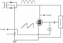
Basically, but it needs all the extra CCS stuff mentioned earlier to DC bias the Mosfet, without loading down the screen or plate for the tracer accuracy. The Y output would still be plate (+screen) current as usual for plate curves (from the current sense R), unless you just want to see the screen V.
Looking at your tracer setup, it appears there could be a simpler way to measure the plate + screen current. What if the bottom of the divider gets moved over to the top of the current sense R? Then the R divider current is removed from the output display, but the screen current is still summed with the plate current thru the power supply.
Looking at your tracer setup, it appears there could be a simpler way to measure the plate + screen current. What if the bottom of the divider gets moved over to the top of the current sense R? Then the R divider current is removed from the output display, but the screen current is still summed with the plate current thru the power supply.
Last edited:
For the plate V to go below the screen V, you will need the CCS on the Mosfet follower drain, to a B+ (and the cap from drain over to the plate). Normally a DC B+, but here that causes problems with screen current occuring while the plate V is zero (although limited by the CCS at least). Could try connecting the CCS to the rectified plate AC with maybe a resistor down from there to the actual plate to give the CCS some operating delta V. (have to position your plate V pickoff for the tracer horiz. correctly then.)
If you do use a separate B+ for the CCS to the drain, it could be returned to the bottom of the plate current sense R to eliminate that offset. You may be able to then just use a simple R pull-up for the drain, since the variable current thru it doesn't register on the current sense R that way.
Yeah, looks like that is the easiest way, no CCS at all. Just a resistor pull-up on the drain to a separate B+ supply. Then the resistor pull-down, from the Mosfet source, goes to the bottom of the plate current sense R too, so it doesn't register either. Only the screen current actually going thru the plate supply return path registers thru the sense R.
Obsolete comments:
A simple resistive pull-down on the Mosfet source could similarly (to the R divider) just go to the top of the (plate) current sense R to eliminate the Mosfet current effect (beyond the screen current) on the tracer display. I think, still trying to figure where the extra CCS current goes then. No, not working, the extra CCS current will dump across the coupling cap to the plate? Or is it? Maybe that current loop (around the CCS loop essentially) doesn't disturb the operation. Will shift the plate V a little, but the tracer pickup is just monitoring the actual plate V anyway.
Last edited:
- Status
- This old topic is closed. If you want to reopen this topic, contact a moderator using the "Report Post" button.
- Home
- Amplifiers
- Tubes / Valves
- To vary a signal pentode to triode in stages