
I have no critics but would like to know why you'd choose some topologies. Why use a currentsource instead of an anode resistor? Why not shift the fase with a tube also? And why do you use 2x2 transistors as outputdrivers? Why not FET's only?
These are no critics, I'd like to learn
These are no critics, I'd like to learn
1) CCS minimize distortion
Not really. The tube is heavily loaded. It doesn't just see the anode resistance where you put the ccs. there is a path through: C3-R10, C3-R14-C8, C3-R14-Q3-.... and the same for the complementary part.
Just putting a ccs anywhere without proper design won't do the job.
so common sense indicates a hybrid power amp.
LOL. Common sense won't get you far in audio. There are a lot of things that SHOULD work but then, they don't. The empirical world is full of surprises. Not that I have anything against solid theory......just saying.
I hate the long tailed pair,
You see?

With Q3 and Q4 current biased like that, I wouldn't expect DC offset to be very stable. The cascodes will reduce self-heating of Q3 and Q4, but can't help with ambient temperature changes etc.
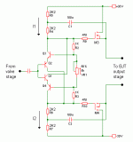
The circuit below may be useful (or at least of interest). It's intended to replace the middle part of your circuit (Q1, Q3, Q4, M1 and M2). M3 and M4 are the same as in your circuit.
How it works is interesting: The DC current I1 through R4 and R5 is always exactly equal to the DC current I2 through R6 and R7 (because there's nowhere else for the current to go), so the output is always biased exactly half-way between the supply rail voltages.
Now what happens if the current gain of Q1 is double the current gain of Q2? The base currents have to be the same, so the current flowing through Q1 and Q4 will be half of the current flowing through Q2 and Q3.
Input impedance is very high, so you should get good linearity from the CCS loaded triode.
Attachments
Last edited:
A CCS minimises distortion provided you don't add a load. You have added a load.popilin said:I'm sorry but I knew a CCS is an ideal load for the valve and mimize distortion, if you have a better implementation of the CCS is wellcome.
Hi the_manta
TubeLib is the Koren lib with other name. Thanks for your interest, if you can, help me please.
Hi godfrey
Thanks for your help, Q1 is in the same heatsink with output transistors, Q3-M1, Q4-M2, M3-M4 has their own heatsink.
I tried gyrators, but the frecuency responce was a disaster, I think to put a CCS at the input of SS stage for bias. (I'm afraid DF96 critics for this)
I tested (a month ago) the topology that you post with poor results, but I will try again, your circuit is a bit different.
I'm afraid of C1-C2, is possible some feedback?
Hi DF96
Thanks for your critics, you are a complete scientist and I respect and appreciate your advice, can you help me with a better idea?
Thanks all
Johann
Last edited:
C1 and C2 are "bootstrap" capacitors. They keep the voltage across R4 and R6 almost constant, by supplying the AC current for R5 and R7. This means the signal current through Q1, Q2, Q3 and Q4 is very low, and the input impedance of the circuit is very high.I tested (a month ago) the topology that you post with poor results, but I will try again, your circuit is a bit different.
I'm afraid of C1-C2, is possible some feedback?
It is a kind of positive feedback, yes.
Well, it's got a buffer, but with an input impedance of about 50K//100pF. The circuit I offered is a buffer/Vbe multiplier with much higher input impedance.Add a buffer?
Last edited:
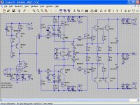
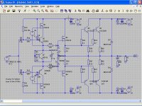
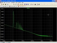
The distortion of SS stage is 0.03% , and 0.3% for the complete amp.
The current through cascodes is 70mA, through the driver MOSFET 90mA, and through output BJT 625mA.
I'm sorry, but the name of transistors was changed.
Best regards
Johann
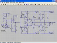
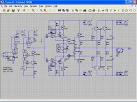
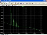
The current through cascodes is 70mA, through the driver MOSFET 90mA, and through output BJT 625mA.
I'm sorry, but the name of transistors was changed.
Best regards
Johann
Attachments
Last edited:
I've only briefly skimmed thru this thread and probably missed some points, but here goes:
Why bjt-mosfet-bjt? Seems to me either single mosfet or three bjts a more logical route. Or have you found that particular combonation best?
I dont see your first circuit such a bad idea, after all the ccs-loaded tube is driving 50kohms, which isnt such a heavy load. (assuming that tube is up to it, I havent checked). Rather that than uneccessary cathode follower.
Sorry, Im on my iPhone so thats all for now. Oh, if only 25watts, why the 40volt rails?
Oh, just looked again and I see the 40v is for your first driver stage.
Last edited:
Hi SemperFi
6BQ5/EL84 is a power pentode with Ra=1K5 in triode connection and I can't see the problem too, but there are forum members that consider 50K a heavy load.
In my country is hard to obtain original transistors, I have 30 2SD669/2SB649 only 5 HITACHI originals, the same with MJE15032/MJE15033, all fakes, nonetheless I have 50 2SA1943/2SC5200 Toshiba originals, I braked two with a hammer to be sure.
The cascode BJT/MOSFET combo helps with thermal runaway, the MOSFET drivers helps with square wave response and avoid the use of another 47pF capacitor.
Thanks for your interest.
Best regards
Johann
- Status
- This old topic is closed. If you want to reopen this topic, contact a moderator using the "Report Post" button.
- Home
- Amplifiers
- Tubes / Valves
- 25W Class A Hybrid Amp