CGS is negligible, for the source follows your gate. There is little energyThe MOSFET has 1300pf Cg so it needs low output impedance to drive, especially when the freq is high. SRPP because the output impedance is low. I think the distortion is acceptable for a hybrid amp. I believe 50% of the distortion is cause by the mosfet. It's a design without global feedback.
stored or released in such a capacitor. SRPP can drive it easily. Capacitor
that worries is CGD! Even though this value might seem small at first.
Miller can be terrible in a MOSFET. Because they conduct so well, we are
tempted to abuse them with low drain voltage. But take away bias that
makes drain capacitance so much less than source? Suddenly, your CGD
cap just got a whole lot larger!!! Worse case, might become a 50/50 split
with the source capacitance. And the effect is multiplied by any voltage
gain...
Keep 10V or more upon your drain, nothing bad is going to happen.
You don't have to worry 1300pF, so long as drain bais shoves most of
that problem to the source end of things, where it can do less harm.
Last edited:
Thanks Kenpeter. I'll redesign the circuit and simulate it with pspice. When the new PCB is fab out I'll send you one kit for testing, thanks for your help.
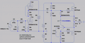
Something like this....
Top MOSFET and voltage divider set voltage.
Bottom MOSFET and current sensors set the
current, and current balance.
The sum of currents sensed by R5 + R6 will
mate for equal and opposite class A currents.
With a fixed total that does not fight itself.
MOSFETs don't need to match, only R5 R6 do...
SRPP is not battling against collector Q1,
Collector is working in your favor this time...
BJT wont be driven to saturation nor cutoff.
Won't hear Q1 struggle to recover anymore.
Ferrite bead prevents possible oscillation.
M1 does not need a bootstrap. C1 provides
the ability for drive to briefly exceed the rail.
Keep 10V or more upon your drain, nothing bad is going to happen.
You don't have to worry 1300pF, so long as drain bais shoves most of
that problem to the source end of things, where it can do less harm.
Does that mean higher supply voltage will make the performance better? My testing result is: THD is 0.05% when Vp-p is 1V, but when Vp-p increased to 5V, THD raise to 0.27%. The supply is +-15V.
MOSFETs switch exceptionally well at low drain voltages, just capacitance
won't stay put where you would like (nor expect) for low-volt linear purpose.
Hard to say a thing with gain won't oscillate, when you don't know from one
moment to the next, to which end of your capacitance might shift???
But your application is unity gain follower. Plenty of local feedback assures
the source voltage has little freedom to deviate. Miller cap trying to squirm
back and forth from source to drain end at low volts is a managable problem.
So long as you don't attempt to make voltage gain with your MOSFETs,
I think low voltage capacitance misbehavior can be adequately controlled.
Its a matter of brute force, unity gain follower conveniently provides...
Yes, higher supply voltage could make the cap behave better. But more
is never enough. Some fool will just crank up the volume, till drain bias
problems return. Gotta enforce your linearity, even in that worst case...
Last edited:
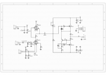
Redesign of circuit
Redisigned a new circuit, it's attached.
Did some simulation with LTspice for the MOSFET part of the hybrid amp. The previous circuit has -48dB 2nd harmonic while the new version has only -62dB, much less distortion. PCB will arrive on Friday, hope there's a better result. My target is <0.1% THD for the entire circuit.
Attachments
Last edited:
")
If we assume both mosfet Sources follow the plate with near zero source impedance,
and 0.7V offset between them: We can compute 0.7V/0.4R = 1.75A quiescent current.
We can also compute the output impedance as 0.2R PAR 0.2R = 0.1R.
And the damping factor probably 8R / 0.1R = 80.
This might be slightly off if the source impedances aren't negligible, and I have not
done any calculations yet to determine the truth or fiction of that assumption.
If we assume 1.75A quiescent: Then positive and negative peaks would be 3.5A?
This implies at least 28V rails into an 8 ohm resistive load. And we probably want
to tack on another 7V or so to keep the drains of our MOSFETs from becoming
big capacitors (at 0V they are same cap as source). I think 35V rails make sense...
And power supplies than can deliver 3.5A on 50% duty cycle = 2A with a big cap...
The biggest challenge to safe operating area will be at 1/2 full rail voltage = 17.5V.
there we will also see 2.19A. And these multiply to 38.3W instantaneous peak power
in each output device. 50% duty cycle means the an average no higher than 19.2W
that each device needs to heatsink away....
Our 3.5A current limit means that 4 ohms loads won't get any louder...
Our 28V rails (plus 7V for drain bias) means that 16 ohms won't get any louder...
So, you ideally do want about 6 to 12 ohm load with this configuration.
Last edited:
The source impedance of the N mosfet is 1 / 6.9S = 0.145R
Because it gets a boost from the BJT, the source impedance
of the P mosfet is probably close to zero. But effectively the
same 0.145R as our N, because it is a copy of the N source.
And not a direct zero ohm copy of the plate. This means our
load is still centered properly in the middle.
New output impedance with source impedance included is 0.17R,
and the new damping factor 46.4
------------
With any SRPP you want the load centered in the middle of the
current sensing resistor. And our output stage is also an SRPP
(unity gain and upside down), but SRPP none the less...
The triode SRPP is loaded at the top end of its sense resistor,
and this is not a mistake. Cathode impedance is not negligible.
Midpoint with cathode resistance figured in, is probably close
to the cathode (if not somewhere inside the triode where you
can't get at it anyways)...
Last edited:
Whoops! My earlier dissipation figures were based upon class AB math.
This output stage is class A, and max dissipation would be at quiescent.
1.75A * 35V = 61.25W per output device! And no breaks for 50% duty.
(You could trick it to be square law Class AB amp. Replace output sense
resistors with Schottky diodes, and shunt maybe 33R across Q1's VBE to
assure 20mA minimum flows at all times. Silicon Schottky diodes rated
for about 5A would probably give the right curves to cross like a 6L6.
I'm not saying this would sound any better, just idle a lot less hot...)
Last edited:
My simulation suggests the remaining distortion might be the triodes?
I'll suggest a fix for that later, when I've determined an optimum bias.
You have floated the heaters to 83V, suggesting an intent to split the
supply voltage equally? But then put unequal cathode resistors to bring
the upper cathode down to 83V??? I think the upper cathode needs to
be at 125V. And the filaments are probably fine at 83V as they are.
It only seems more linear with 2K2 than 470 up there because current
is more constant with 2K2. But this low distortion has many high order
spurs. There is a way to have equal voltage split, low spurs, and keep
the higher impedance current source. I'll draw later.
For now, this sim is as much like your schematic as I could fake it.
Some PS caps not drawn, and I didn't have a .model for BC560 PNP.
Attachments
2K2 is fine, I was thinking MORE, like 10K. In series with 470 for bias...
Then 100 K grid leak to bottom of 470, and 470n coupling cap from grid
of T1B down to the bottom of the 10K.
Duncan Amps has the triode models.
http://www.duncanamps.com/spicevalvesgt.html
Its the first one, the Pspice model. Works fine in LT.
Then 100 K grid leak to bottom of 470, and 470n coupling cap from grid
of T1B down to the bottom of the 10K.
Duncan Amps has the triode models.
http://www.duncanamps.com/spicevalvesgt.html
Its the first one, the Pspice model. Works fine in LT.
Last edited:
So, 10K proved maybe a bit much. Stole too much voltage.
A mere 4K7 steals 36Volts! But the current is indeed stiffer.
Really hard to wring a good result out of 250V split halfway.
And any more voltage might want filaments too far apart...
Trying to bias for best compromise: 7mA @ 850mW per plate
was about the highest I could manage without risking forward
grid current into T1A.
Gain is up somewhat closer to Mu, due to the stiffer current,
and also due reduced R6 degeneration at the cathode of T1A.
I had to reduce input slightly to compare same output level.
If you wanted even more Mu gain and less degeneration? An
LED rated 1.7V at 7mA might do for R6. Puts sand in voltage
gain path though, maybe not so appealing to triode purists.
http://www.dialight.com/Assets/Drawings/2D_Drawings_DrawingDetailedSpec/C17441.pdf
Attachments
Last edited:
A JFET that passes 7mA might also be interesting for R5...
Since C3B couples around it, its not really in the signal path.
http://www.centralsemi.com/engineering/spicemodels/spicecld.aspx
Closest current limiting diode (2 lead JFET) with spice model
I find so far: is rated 5.7mA, maybe close enough? Less than
7mA is OK, more than 7mA and you risk drawing grid current...
Last edited:
I tested the new circuit today. THD drops to 0.08%, very good result!
An externally hosted image should be here but it was not working when we last tested it.
Last edited:
Sorry, photo is missing...Here it is:
An externally hosted image should be here but it was not working when we last tested it.
- Status
- This old topic is closed. If you want to reopen this topic, contact a moderator using the "Report Post" button.
- Home
- Amplifiers
- Tubes / Valves
- Playing with hybrid amp: SRPP + MOSFET