Hullo all,
So I've been using my spare time recently to try to go from school physics to valve design, namely an AB1 amplifier using 6S41S valves, mainly because I think they look good and feel a bit different.
Trying to collate all the huge number of things has been rather mind-numbing, but I hope I'm getting there.
The idea was to have full output from 1.4Vrms and use the excess gain for NFB when I've read up on it, so it's not included yet - besides the whole circuit might be ridiculous to more experienced eyes, so any feedback (ho ho) gratefully received.
Originally I had 12S3Ss for the mu-follower but there wasn't enough H.T. to give them the necessary swing, so I chose the 6S45P-E. I've not calculated for anything beyond the output stage yet. The quiescent point of the 6S41s I've put at 210V/80mA at 1.2K (-80Vg).
Last edited by a moderator:
I've been going back through this now more time has become available, and am trying to work out how I got to where I was. When faced with pages of old calculations, it's hard to get back in the same mindframe!
I'm now wondering if a two stage driver of 12S3S would provide the necessary swing for the 6S41S output stage.
How do you folks go about it? Morgan Jones appears to favour going from input to output, but some of my old Wireless World articles explain a method going from the output requirements backwards...
I am investigating if 6N1P > 6N1P Phase Splitter > 12S3S > 12S3S > 6S41S is feasible.
...I'm now wondering if a two stage driver of 12S3S would provide the necessary swing for the 6S41S output stage.
You need some 160 Vpp or more driving voltage for 6S41S output stage.
The only solution to generate this level is to have sufficient supply voltage for the driver stage.
With 210 V +Ub it is not possible to get with normal circuits, but by taking the in-phase bootstrapped supply voltage from the anodes of the output tubes it may work.
I have built PP amplifier with 6AS7G that reguired 240 Vpp drive voltage.
My solution was to have high 380 Vdc supply voltage for the driver.
Thank you artosalo.
I am away this weekend, so can't consult my calculations, but I *think* I had 120Vpp required.
I will post my working out when I return, and see if I have made a mistake somewhere. I will remove the above sketch layout, as I have changed it since I posted but need to contact an administrator as it is so old!
Do you work backwards from the output or forwards from the input when designing amplifiers?
Do you work backwards from the output or forwards from the input when designing amplifiers?
It's incomprehensible to me, how anyone could design a power amplifier starting with the input stage. The usual starting point is a specification for power output and performance level, which leads directly to output stage design, and then to driver stage design, which cannot proceed until power stage drive requirements are known. The whole process devolves somewhere beyond that point because there are so many interdependencies on power supply, budget, reliability, component availability, and the designer's skillset.
In the DIY world, the starting point might be whatever components happen to fall into the designer's hands, or a circuit concept that begs investigation. My most recent design was motivated by a desire to create something with good performance around 20 watts per channel that could be constructed by other folks at very low cost, and using only components that should remain available for a long while.
It's incomprehensible to me, how anyone could design a power amplifier starting with the input stage.
I do not recall that Jones mentioned "design from the input to the output", perhaps the OP can provide an exact reference of where that came from...
Thanks for the replies.
BinaryMike, I hear you on 'whatever components happen to fall into the designer's hands' - those boxes of parts seem to accumulate!
jazbo8 - perhaps I misremembered him. I'm sorry for the delay, work has kept me away from home unexpectedly. I shall post a reference (if there is one) on my return, along with the promised calculations.
I do not recall that Jones mentioned "design from the input to the output", perhaps the OP can provide an exact reference of where that came from...
Having now had a pretty comprehensive scan through Mr Jones's opus, I can't find the reference so I am going to put it down to mis-remembrance. It did seem at odds with common sense, so that's cleared up one sticking-point for me!
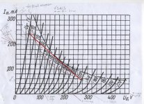
Before posting the rest of my output calculations, I ought to check I'm on the right track. Here're the results of my push-pull loadline sums, for power dissipation and output so I hope they make sense to more experienced eyes. Please excuse my mind-jogging explanatory sentences.
I have omitted my mirrored push-pull loadlines for clarity.
from loadline based on a load of 1K2 Ohms per 1/4 phase, Vpp = 340V.
DC current (Ipq)= 58mA therefore anode power dissipation = Vpp*Ipq = 340*58E-3 = 19.72W
The maximum dissipation of the anodes is 25W from the valve data sheet.
To find the output power (Po) we need the peak current from the loadline at Vgk= 0, Ipeak = 244mA.
Irms = 244E-3/sqrt2 = 173mA
Po = 173E-3*1.2E3 = 35.9W
to find the total DC anode input power (Pdc)
Iave= 2(244E-3)/pi = 155mA
Pdc = 340*155E-3 = 52.81W
Pd = (52.8-35.9)/2 = 8.5W
Attachments
- Status
- This old topic is closed. If you want to reopen this topic, contact a moderator using the "Report Post" button.
- Home
- Amplifiers
- Tubes / Valves
- First try P-P 6S41S design