Hi all,
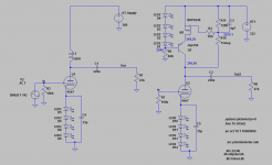
I'm in the process of optimising my 6J5 driver which currently has a CCS load.
Based on Wavebourn's circuit, I calculated the version to set the 6J5 at Va=260V and similar frequency response equivalent to a 150H ideal choke.
When I breadboarded the circuit, couldn't make it work. Although at some point I burned the LED array and got it biased properly by sheer luck. When I replaced back the LEDs, still couldn't make it work.
The PMOS is actually an FQP3P50, but couldn't find an LTSPICE model for it. I guess will have an impact on AC due to different capacitance, but should respond similar in DC? Haven't compared characteristics though....
The values I measured are in blue. Not sure about the value of the gate voltage as it's difficult to measure it with a voltmeter. When probe is connected it affects the impedance and then LEDs turn off until probe is removed - is this ok?
R11 is actually two 1M in parallel plus a 220K preset. R10 is two 22Meg in parallel.
The MJE350 emitter voltage should be at 324V, not the value highlighted.
Any suggestions where the problem could be?
Attachments
Hi Ale,
The circuit (as drawn) can't work, I fear.
The LEDs will make the MJE circuit into a CCS only if the MJE350 can force about 324.6V on its emitter. With 316V on the emitter, the MJE350 will be degraded or destroyed, so you'll need a new one, sadly. See the specification for Veb(max), usually 6.0V.
Please post the Wavebourne original - I think the FET should be the other side of the MJE350 - to set the cascode voltage according to the stabilised voltage at the anode.
Hi Rod,
Yes, I thought the VCE measured might have killed the MJE350.
I think the circuit is ok, albeit my adaptation is not....see this thread:
http://www.diyaudio.com/forums/tubes-valves/140699-anti-triode-sepp-how-do-best-9.html
Thanks for the help
Ale
Yes, I thought the VCE measured might have killed the MJE350.
I think the circuit is ok, albeit my adaptation is not....see this thread:
http://www.diyaudio.com/forums/tubes-valves/140699-anti-triode-sepp-how-do-best-9.html
Thanks for the help
Ale
The most important omission is a resistor between the P-FET source, and the +ve supply. This sets the current for the triode's anode circuit.
The value is found from the voltage across R11 minus the Vgs of the P-FET, divided by the current you want to see in the anode. The voltage across R11 should be 10 - 20V for stable operation.
Next the cascode voltage needs to increase. This should be roughly (voltage across R11 + 10V), or 25 - 30V as a starting point. This will make sure the P-FET has enough headroom to stabilise the current.
If you omit the source resistor, the programmed current will be unstable, and always much larger than the triode can handle.
Concrete example:
If you adjust R11 to have 10V across it, and we assume the FET Vgs is 4V, then the source resistor must be 600 ohms to get 10mA, 300 Ohm for 20mA .. all the way up to 2000mA for 3 ohms! This will be independent of supply voltage. You can see that a source resistor of zero is not possible.
However, you will not get any current at all unless the MJE base is lower voltage than the FET gate - probably 10V lower, for stable results.
The simulation must work correctly even if the supply voltage is changed by 30V in either direction. If it does not, the circuit will not be stable in practice.
I cant see how that layout could possibly work anyway!
Where is the signal at the plate being developed and used as the input to the MOSFET?
--Its effectively removed by the 4.7uF cap!
Nah, I prefer a straightforward and highly effective single MOSFET, plate resistor, coupling-cap and pot. divider to set op.-point....
Super Simple, Great Performer....
Where is the signal at the plate being developed and used as the input to the MOSFET?
--Its effectively removed by the 4.7uF cap!
Nah, I prefer a straightforward and highly effective single MOSFET, plate resistor, coupling-cap and pot. divider to set op.-point....
Super Simple, Great Performer....
I cant see how that layout could possibly work anyway!
Where is the signal at the plate being developed and used as the input to the MOSFET?
--Its effectively removed by the 4.7uF cap!
Nah, I prefer a straightforward and highly effective single MOSFET, plate resistor, coupling-cap and pot. divider to set op.-point....
Super Simple, Great Performer....
Not that great. Any uncompensated semiconductor CCS is going to drift all over with temp

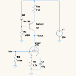
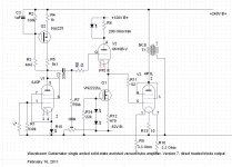
Try a setup like the one I attached. Rcs sets the current through the tube, while Rb sets the bias, and hence the quiescent voltage across the tube. D1 compensates against temp changes, thus keeping the current relatively stable over temp. Do NOT use the D45H11 - I just picked it for an example. It doesnt have the voltage rating for this circuit. Pick a transistor with Vce equivalent to your supply voltage and with an hfe as high as possible (but NOT a darlington!).
You notice that I used a resistor in the cathode circuit rather than LED's. The reason is that diodes are essentially a fixed bias, which will make the circuit sensitive to the characteristics of the tube. This is a Bad Thing™. You want the circuit to be as insensitive as possible to variations between individual tubes (and semiconductors). That is why a resistor is used to set the bias, as well as in the emitter circuit of Q1 to set the current (rather than using a divider in the base circuit). Also, depending on the characteristics of the diode and transistor there may not be enough voltage across D1 to forward bias Q1. If that happens, add some resistance between D1 and the base of Q1 . Do not add another diode or a transistor with the base tied to the emitter of Q1 like you see in a lot of SS circuits as it will screw up the temp balance. You can replace D1 with another transistor identical to Q2 with it's base tied to it's collector. In that case the emitter goes to B+ and the collector to the junction of Q1's base and R2. Provided both transistors come from the same wafer lot it will give you the best thermal tracking.
Attachments
Last edited:
If you omit the source resistor, the programmed current will be unstable, and always much larger than the triode can handle.
Concrete example:
If you adjust R11 to have 10V across it, and we assume the FET Vgs is 4V, then the source resistor must be 600 ohms to get 10mA, 300 Ohm for 20mA .. all the way up to 2000mA for 3 ohms! This will be independent of supply voltage. You can see that a source resistor of zero is not possible.
However, you will not get any current at all unless the MJE base is lower voltage than the FET gate - probably 10V lower, for stable results.
The simulation must work correctly even if the supply voltage is changed by 30V in either direction. If it does not, the circuit will not be stable in practice.
Hi Rod,
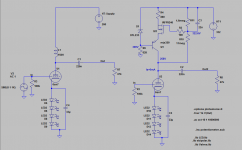
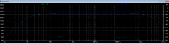
Thanks for the help. Attached is an updated simulation. Have changed the LED array for a simple 33V zener to get the cascode voltage down to 300V - if I got it right from your suggestion above. Added the source resistor to set divider voltage as recommended and get the quiescent current to around 6mA. What it puzzles me now is that I need to reduce significantly the capacitor to 22nF to achieve the LP corner at 15Hz equivalent to the 150H inductor. From what I was reading in the thread mentioned before, the value should be higher that 1u at least.
What is driving the low frequency response then?
Thanks again for the help, I'm learning a lot with all this!
Cheers,
Ale
Attachments
I cant see how that layout could possibly work anyway!
Where is the signal at the plate being developed and used as the input to the MOSFET?
--Its effectively removed by the 4.7uF cap!
Nah, I prefer a straightforward and highly effective single MOSFET, plate resistor, coupling-cap and pot. divider to set op.-point....
Super Simple, Great Performer....
Is this not the principle of the gyrator circuit? You want a fixed voltage in DC as would an ideal inductor provide, and then a high impedance response at high frequency.
What gyrator circuit do you recommend?
On a separate note, I tried multiple CCS configurations with excellent results!
Not that great. Any uncompensated semiconductor CCS is going to drift all over with temp
Try a setup like the one I attached. Rcs sets the current through the tube, while Rb sets the bias, and hence the quiescent voltage across the tube. D1 compensates against temp changes, thus keeping the current relatively stable over temp. Do NOT use the D45H11 - I just picked it for an example. It doesnt have the voltage rating for this circuit. Pick a transistor with Vce equivalent to your supply voltage and with an hfe as high as possible (but NOT a darlington!).
You notice that I used a resistor in the cathode circuit rather than LED's. The reason is that diodes are essentially a fixed bias, which will make the circuit sensitive to the characteristics of the tube. This is a Bad Thing™. You want the circuit to be as insensitive as possible to variations between individual tubes (and semiconductors). That is why a resistor is used to set the bias, as well as in the emitter circuit of Q1 to set the current (rather than using a divider in the base circuit). Also, depending on the characteristics of the diode and transistor there may not be enough voltage across D1 to forward bias Q1. If that happens, add some resistance between D1 and the base of Q1 . Do not add another diode or a transistor with the base tied to the emitter of Q1 like you see in a lot of SS circuits as it will screw up the temp balance. You can replace D1 with another transistor identical to Q2 with it's base tied to it's collector. In that case the emitter goes to B+ and the collector to the junction of Q1's base and R2. Provided both transistors come from the same wafer lot it will give you the best thermal tracking.
Very interesting comments. The gyrator in theory tackles the variation of valves and aging by setting a fixed voltage, not like the CCS which sets a fixed current.
I think that the 1uF is a good idea. The LF pole is formed from the M-ohm level gate resistors against the cap.
The 1uF is useful:
1. because the LF response can be lower, minimizing the risk of phase changes accumulating across all the stages in your system. This can be an advantage over the choke.
2. The 11M resistor is potentially too high. I know it simulates OK, but the gate leakage from a MOSFET can be as high as 1uA.... probably won't be but the high impedance can be a problem for other reasons. Anatolij used 4,3M elsewhere, and that seems safer to me.
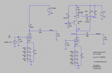
Makes sense then to reduce it. See simulation attached. I guess that you would prefer a MOSFET with lower input capacitance as this will be in parallel with the capacitor and influence the frequency response?
With a 4.7Meg resistor and 1uF capacitor the response is nearly equivalent to a 500H choke! Nice...
Thanks
Ale
With a 4.7Meg resistor and 1uF capacitor the response is nearly equivalent to a 500H choke! Nice...
Thanks
Ale
Attachments
Maybe Anatolij (Wavebourn) is on holiday - I am surprised he has not appeared, and explained (and defended) his circuit.
It's pretty neat, actually. I hope he won't mind if I try to explain.
I think it is easier to understand its workings if we look at his Губернатор-7 (Gubernator-7) design. This is a robust design for Russian tubes 6Ж5П - 4П1Л (6J5 to 4P1L) SE power amp. It tolerates very well the wide variation between samples of the 6Ж5П - a useful feature for any amp.
The 6Ж5П stage uses the Gyrator circuit to automatically find an operating point. The anode voltage programmes the gyrator current (dc-only) through R2-R3. Meanwhile the cathode circuit is fixed-bias (~1,5V) - but this does not prevent the circuit from self-stabilising. You could pull out the 6Ж5П and use another one (with VERY different Ia-Vg1 characteristics) and the Gyrator will find a suitable operating point. The same process compensates for aging in the 6Ж5П - say for instance the anode current falls over time - the gyrator will increase the dc anode voltage to compensate.
At the same time, the fixed bias in the cathode eliminates the cathode capacitor - a well-known weakness in any design.
This is a very well designed circuit that gives EXCELLENT performance, perfectly stable dc operating conditions, high stage gain - and yet all the components are dirt cheap.
The version of Gyrator you are working with is cascoded, too, which may increase the performance (and power supply rejection) even further.
Attachments
I guess that you would prefer a MOSFET with lower input capacitance as this will be in parallel with the capacitor and influence the frequency response?
Hi Ale,
It's worth choosing the P-FET carefully, because the drain-source capacitance [Coss] varies very much. according to the size of the FET. Low capacitance means better HF power supply rejection, and which amp could afford to turn down such an offer?
The 33V cascode diode can also help. When you choose your FET, look at the Coss Vs. Vds graph. Then make a 3-way tradeoff between FET dissipation (big FET needed), low 30V capacitance (small FET needed) and the anode-voltage swing required (low diode voltage needed).
Maybe start by looking at the Gubernator's BSP225, and compare other FETs to that.
Ok, the BSP225 has a Coss of 20pF whilst the FQP3P50 has 70pF! The big difference is on the CiSS (65pF against 510pF of the latter). How does the CiSS impacts in this circuit? Is it shunt capacitance in parallel with the 1uF capacitor?
When you refered to the diode characteristics, did you mean looking for a zener with low capacitance, correct?
I guess that if I want to use the BSP225 will need to learn how to solder an SMD device!
cheers,
Ale
When you refered to the diode characteristics, did you mean looking for a zener with low capacitance, correct?
I guess that if I want to use the BSP225 will need to learn how to solder an SMD device!
cheers,
Ale
Coss of 20pF (please check what voltage - often 25V) - that's hard to beat.
Ciss is no worry, it's in parallel to the 1uF, as you noted.
I was thinking only about changing the diode voltage - sometimes there's a sharp improvement in Coss for a small increase in Vds.
SMD soldering is a piece of cake, provided you get some solder paste (Edsyn syringe, from Farnell)
Ciss is no worry, it's in parallel to the 1uF, as you noted.
I was thinking only about changing the diode voltage - sometimes there's a sharp improvement in Coss for a small increase in Vds.
SMD soldering is a piece of cake, provided you get some solder paste (Edsyn syringe, from Farnell)
Voltage Drift of the MOSFET scheme I used is not a probem....
Since it was mentioned, I tested. From stone-cold to fully hot (after 2 hours and tested 4 different CCS Stages in same amp)
--Voltage 'drift' was less than 2V at MOSFET....
--I think that was more mains supply variation than anything to do with the semi-device!
So, better than 1%
Voltage-drift isnt an issue.
--A personal thing--I DONT like Bi-Polar transistors!
Here is the idea I used, check out near bottom of paper--
Mu Stage Philosophy © 1993 Alan Kimmel
Last edited:
Maybe Anatolij (Wavebourn) is on holiday - I am surprised he has not appeared, and explained (and defended) his circuit.
It's pretty neat, actually. I hope he won't mind if I try to explain.
A CCS by any other name still does the same thing
And the use of a fixed bias will still make the circuit sensitive to variations between tubes.- Status
- This old topic is closed. If you want to reopen this topic, contact a moderator using the "Report Post" button.
- Home
- Amplifiers
- Tubes / Valves
- Help with gyrator