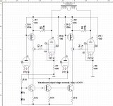
Thinking about power amp without coupling capacitors, with local feedbacks around output tubes, I come to some interesting solution.
Everything is DC coupled, input capacitances of MOSFETs are bootstrapped by feedback from anodes of output tubes, and their bias depends on stability of current sources in the negative rail of power. When tubes start, or some of them dies, everything else is fine. It is safe amp, not self-destructive.
Looks like some nice new construction.
Was it patented by somebody before, or not yet?
The schematic is a bit incomplete: I could not draw more because free version of Rimu Schematic software limits number of elements on the drawing.
Attachments
Hey A,
Interesting idea. Still it doesn´t make sense to me.
Iq for the left MOSFET is set by R1. Then you have a current-source where current is set by R13 at the bottom that also should set Ig.
If I for some reason should be right, one might substitute the CCS with a gyrator?
Ooops Kenpeter, our posts crossed;-)!
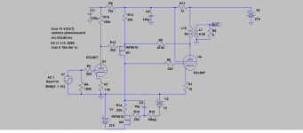
EDIT: Maybe something like this as SE?
Interesting idea. Still it doesn´t make sense to me.
Iq for the left MOSFET is set by R1. Then you have a current-source where current is set by R13 at the bottom that also should set Ig.
If I for some reason should be right, one might substitute the CCS with a gyrator?
Ooops Kenpeter, our posts crossed;-)!
EDIT: Maybe something like this as SE?
Attachments
Last edited:
I think the feedback amount for this setup will be very low due to the Mosfet source impedance being so low. Basically becomes current thru the feedback resistor versus the delta-Vgate*MosfetGm. But then the Mosfet forward gain (CCS loaded drain) increases the loop gain enormously to compensate. Still, the bias point will not be stable against Mosfet temperature drift due to the huge gain at the Drain. Revintage's gyrator looks to be necessary.
I have modeled a somewhat similar circuit that uses the P channel Mosfet similarly, but instead of input signal driving its gate, I made the bottom drain-loading-CCS a driving pentode. I thought of it more along the line of a modulated CCS load (the P Mosfet) for the driving pentode. The pentode current then has to equal the modulated CCS current, with large loop gain available (CCS versus pentode current) to make it so. An additional stabilizing feedback (not temp. sensitive) went back to the driving pentode screen grid.
I have modeled a somewhat similar circuit that uses the P channel Mosfet similarly, but instead of input signal driving its gate, I made the bottom drain-loading-CCS a driving pentode. I thought of it more along the line of a modulated CCS load (the P Mosfet) for the driving pentode. The pentode current then has to equal the modulated CCS current, with large loop gain available (CCS versus pentode current) to make it so. An additional stabilizing feedback (not temp. sensitive) went back to the driving pentode screen grid.
The feedback to the Mosfet source is tracking the gate input signal, so should increase the input Z (so lowering Cinput). Crss from drain to gate would be important though. P channel parts also have the worst capacitance specs. Another issue is the high impedance that is driving the output grid, but feedback controls that (at least for tube turn on, but not for turn off).
Last edited:
The problem should be the input capacitance of the MOSFET.
That's why it should be better to use P-type tube than MOSFET.
")
That's why it should be better to use P-type tube than MOSFET.
But seriously, with a decent driver like E88CC, Fu will be in the ballpark of 75kHz with IRF9610.
The feedback to the Mosfet source is tracking the gate input signal, so should increase the input Z (so lowering Cinput). Crss from drain to gate would be important though. P channel parts also have the worst capacitance specs. Another issue is the high impedance that is driving the output grid, but feedback controls that (at least for tube turn on, but not for turn off).
Whatever causes it, hf-response sucks.
Last edited:
I dont see where they forgive each other to agree a quiescent current?
Values of R1 and R11. But gyrator is a good idea as well, more stable.
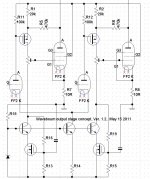
The resistors or Zeners go just above the trimpots. No need for the Mosfet(s) to drop nearly all of the B+ (more than B+ actually, due to inductive primary swing), they just have to swing enough for the output tube grid drive. Gonna want some zener gate protection on the Mosfet(s) for when the output swings above B+. If you put an inductor load on the first triode tube(s) as well, then the gate and source can swing together above B+. With the resistor loads on the triodes as is, you may need to provide a boosted B+ for them, so that the Mosfets can turn off when the primary output swings above B+.
Connecting the tube cathodes together (resistor feedback of output current, cath. to cath.) for SE would raise the output Z. Unless you put the xfmr secondary below the output tube cathode to get neg. voltage feedback.
Connecting the tube cathodes together (resistor feedback of output current, cath. to cath.) for SE would raise the output Z. Unless you put the xfmr secondary below the output tube cathode to get neg. voltage feedback.
Last edited:
Oh, a DC servo like loop.
The Miller capacitance of the driver Mosfet could be largely eliminated (for easier drive by the triode) by using a cascode Mosfet below the existing one.
Then can also use a lower voltage part for the control Mosfet, if parameters are better. Or, allows one to split the big voltage drop down to the output grid in half too.
Oh, a DC servo like loop.
Yep. A common cathode resistor shunted by a cap.
The Miller capacitance of the driver Mosfet could be largely eliminated (for easier drive by the triode) by using a cascode Mosfet below the existing one.
Then can also use a lower voltage part for the control Mosfet, if parameters are better. Or, allows one to split the big voltage drop down to the output grid in half too.
Right, and something small like BSP225 can be used.
The signal inversion, due to the Mosfet driver stage, allows one to use a second resistive divider local feedback from the output tube plate back to the input tube g2 (now a pentode), without having to use crossed feedbacks. Giving, effectively, single triode response from signal input to OT, with no coupling caps. The input tube plate and g2 voltages can track (depending on attenuation ratios), allowing a resistive linear feedback. The input tubes can be LTP'd for P-P splitting or the scheme works for SE too. The very high gain at the Mosfet driver drain could work well for g2 drive of the output stage as well (using an additional Mosfet follower for the output tube g2 to maintain constant current operation of the Mosfet driver). Or even a scaled g2/g1 combo drive.
This is definitely looking to be a very useful circuit topology.
The tube purists are going to blow a gasket though if we don't come up with a P-tube.
Here's a first crack at that: In place of the driver Mosfet, we put a normal pentode with plate at the source connection to the 20K pullup, screen grid at the 470K feedback connection, and cathode at the drain connection (to output g1). Input from the 1st tube gets applied at its g1. Gyrator is still pulling down on the cathode. The pentode gets biased to drop the required volts from plate down to the output stage grid1. The loop no longer has the high gain provided by the Mosfet, but we can make up for that by using a CCS as the plate pullup for the input tube. The above scheme (pentode input tube, g2 feedback) now comes into play to provide the very high loop gain needed for the feedback loop. (high gain comes from the CCS loading of the input pentode) So we have just moved the loop gain up to the 1st stage instead of the middle stage.
Last edited:
(ran out of edit time, continued
The middle pentode, which now replaces the Mosfet, is able to maintain the constant current flow mandated by the gyrator only if the screen g2 voltage (from the feedback) varies as its internal triode Mu times the input g1 signal.
The whole tube is effectively suspended by high Z at both its plate (its own high Z plate) and cathode (gyrator), only gyrator current rules its operation. Output, as seen by the screen feedback, must be at Mu times the g1 input or the gyrator throws a fit. Not sure how to compute the loop gain there. Maybe output tube gain divided by middle tube Mu? In any case, the input tube, with high gain CCS plate loading and g2 feedback, will have high gain to enforce final output = its Mu times the actual input times any resistive attenuators.
OH, and the 470K feedback resistor will have to be lowered considerably to drive the middle tube g2. And the 20K plate load will have to be reconsidered, maybe just shorted to 0 Ohms.
Last edited:
- Status
- This old topic is closed. If you want to reopen this topic, contact a moderator using the "Report Post" button.
- Home
- Amplifiers
- Tubes / Valves
- New concept of a power amp