Thanks Indra for your help here, much appreciated.
I will try to trace the depletion FETs using the uTracer if possible. This can be very insightful if I can plot the real curves for the DN2540 to optimise the operating point. I'm hopeful I can minimise the HF distortion this way. It's a very simple circuit and I like the sound of both DN2540 and LND150.
I will still try both jFET and bipolar options. I'm very keen to do a listening test and find out what difference in sound they bring to the party.
I want to test the two options with input capacitor and without deliberately so I can judge the sound of them. If I build a negative supply, I could ground the input resistor of the bipolar and connect the emitter resistor to the negative supply and get rid of the input cap I suppose. Equally, the bias arrangement of the bipolar can be used for the jFET and get rid of the negative supply with the penalty of the input cap.
I could solder the BF862 on to those SMD PCB adaptors, but how can I then build a test rig to measure these? Is there a ZIF socket for the BF862 to build a test rig?
I think I have 2SK170 and still 2SK369 at hand and of course some MPSA42 and BC550 I could use here. Any other suggestions for bipolar/FETs to use?
Thanks
Ale
hi Ale
With MOS, the curves are badly nonlinear, and the gm so low, that degeneration cannot help very much.
If you try JFET, I would avoid BF862 in this position - the breakdown voltage of 20V is too low. Other JFETs might work, but don't forget the protection zener.
With a BJT - even at 1.3mA you have nearly 50mA/V in any old transistor (gm is structural in BJTs, as opposed to depending on type, for J- and MOS- FETs).
This allows us to use degeneration with an emitter resistor, and reduce the distortion.
The attached example shows how you can swing 24V pk-pk wth < 0.4% distortion, high orders well down. I have used 1.3mA of Ic, to match the circuit you've already tried, and keep the burden on the OT as low as can be.
It can be improved further by using another transistor, but I think it will be worth trying this simple circuit.
Many types of NPN transistor will work, but the MPSA42 has low Cob, and 300V durability,so it will survive the usual slips, in development!
Note that a negative supply is used. If you don't, the grid cannot swing to 0V, which is unlikely to work well enough. The negative supply also allows the degeneration-resistor to be selected for best performance, and gets rid of the input cap. so I think you will prefer it.
The sound of BJTs themselves is not bad - it's the badly designed circuits they usually wind up in!
Attachments
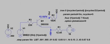
Base Resistor (R3) in above BJT circuit should be 470 ohm.
Distortion much lower with that value.
Also, the frequency response shows about -1dB at 30kHz, with 14pF load. (10pF for 4P1L input, 5pF stray, BJT and Miller accounted for). So the 182K resistor is probably the maximum value to use, and may be the optimum. Distortion increases for lower values.
Distortion much lower with that value.
Also, the frequency response shows about -1dB at 30kHz, with 14pF load. (10pF for 4P1L input, 5pF stray, BJT and Miller accounted for). So the 182K resistor is probably the maximum value to use, and may be the optimum. Distortion increases for lower values.
Hi Ale, I concur with Rod on most points. Especially generalization on a device as a class. Well designed circuit with reasonable care on part selection and OP should not sound bad, they just taste differently. Some do sound really bad compared to others close to and during clipping, but I think discussion of performance on normal listening level is more meaningful.
I prefer the sound of low voltage parts and in my opinion, low voltage parts should not give problems on a well designed circuit. On SSHV1 Salas showed safe use of 2SK170 (rated 40V) on 250V system. But as Rod mentioned, it will not survive a "slip". Protection zener is strongly advised during breadboarding. Perhaps it is more logical to choose high voltage rated parts for high yield production environment, but choice of parts based on sound preference is equally logical for DIY and low yield custom production environment, we just need to understand the pitfalls.
The LND150 should work well operated at 3-7mA with positive Vgs. And I just remember that Mouser have ALD114835, a dual small signal depletion MOSFET, tightly matched at the factory. Maybe you want to add it to your list since you indicate preference to sound of depletion MOS.
ZIF SOT23 sockets are frequently discussed such as in BF862 preamp thread post #306 and #310. You may also try Dave's trick shown at A soldering aid for SMD by Dave g3vze to avoid the expensive ZIF socket. However, due to the high Idss, I think BF861A is a more suitable member to use here compared to BF862.
Here is the list of some small signal parts i have used :
- N-JFET : MPF102, 2SK30A, 2SK68A, 2SK117, 2SK163, 2SK170
- NPN : BC109, MPSA18, MPSL01, 2SC828, 2SC945, 2SC1815, 2SC1845, 2SC2240
However, we live in different part of the world, easily available part selections are wildly different. Rod should be able to give you a better list with easier to obtain parts.
Last edited:
Rod,
I was reading Douglas Self's chapter on VAS amplifier and found out that MPSA42 is quite a good candidate for this application. However, to avoid HF distortion due to Ccb variance, needs to be run with Vcb > 30 or 40V. I'm not sure LTspice will cover this on the NPN model for the MPSA42, but am sure it will come up during measurement.
So I will be inclined to increase collector voltage and readjust the bias of the 4P1L. I was planning to do this anyway for testing again the DN2540.
Why distortion reduced when Rb was reduced? I was expecting a reduction of noise unless you modified the OP of the MPSA42 and is running in an optimal part of the vbe/Ic curve?
I have some ZVN0545 I think so may try that one as well. The bias arrangement suggested looked like the best way of removing the input capacitor as discussed earlier. After all, adding a negative supply here is not a big deal given simplicity of overall amplifier.
Indra,
Great suggestions, many thanks. As said I have LND150 at hand and 2SK170, etc. I may try these first. Plenty to test!
The dual depletion FET looks really good, albeit the VDS max is just 10V
Thanks
Ale
Hi Ale,
Most semiconductors show lower Cout with increased voltage. With MOS it's far more dramatic. With MPSA42 in this little stage it should be fine at 20V or more.
Rb distortion is due to base current (signal current) - the output swings are fairly wide.
For simulation, I have shown the 2N5550 for a good reason - it is plenty near enough to the characteristics of MPSA42, especially Cob, Hfe etc.
the very fine 2N5550
Yes, the Vdsx of ALD is kind of restricting, but the transfer characteristic and matched dual is really hard to resist. I should have mentioned another depletion MOSFET, the BSS126, Vdsx 600V and Idss 7mA could be operated 3-5mA at #859 option 1 at negative Vgs.. . . The dual depletion FET looks really good, albeit the VDS max is just 10V . . .
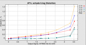
Finally back home after a long trip and had the opportunity to put the DN2540 at test and try the topologies discussed for the “Schade” feedback 4P1L SE amplifier. So I re-build my test rig and tried the DN2540 and LND150 at various drain currents. It was clearly to see that in order to keep distortion to a minimum, the VDS needs to be greater than 60V to keep the output capacitance of the FET low. Here are the results of the frequency response at nearly maximum output power (Po=2W):
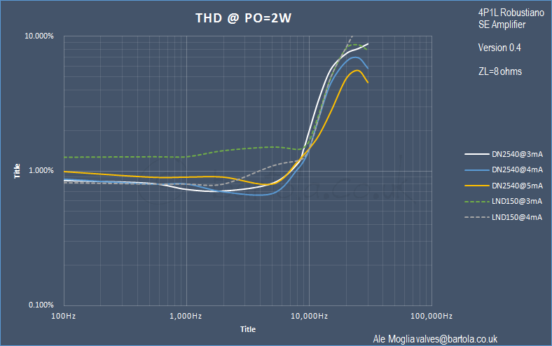
It is interesting to see that the LND150 which has Coss (max) of 3.5pF doesn’t perform much better than the DN2540 which has Coss (max) of about 30pF. Operating points are different for both FETs but the 4P1L is running about the same operating conditions. What is also interesting to verify with this test is that the higher the drain current, the more capability the FET has to drive the 4P1L input (and Coss) capacitance at higher frequencies as the slew rate of the FET is higher.

We can see an interesting improvement from my initial tests at 5mA when drain current was just about 1.5mA. The yellow trace (Id=5mA) shows the best performance of the DN2540. Surely higher drain current will perform better but at a cost as the drain current is part of the OT primary current.
So how do we keep the gain of the FET when increasing the drain current? The natural approach will be to reduce Rf, but this affects the FET gain and the feedback. The alternative is to increase the supply voltage respect to ground. The price we pay here is to increase the cathode resistor and burning the power on it. With -4V as the negative source supply voltage, I had to only reduce RF to 51.5K to set 5mA on the DN2540. The supply power was increased to 350V, the screen (Vg2k) to about 140V (240-98.6V) which is lower than the 150V used before. There is a tad of extra power to extract on the 4P1L but here is close to its maximum dissipation. The Rk is a pair of wirewound 4K7 in parallel.
I think it is now time to try the BJT driver. I suspect that it will need at least 5mA of collector current to get on with the task of the input capacitance of the 4P1L when anode to grid feedback is in place.
cheers
Ale
It is interesting to see that the LND150 which has Coss (max) of 3.5pF doesn’t perform much better than the DN2540 which has Coss (max) of about 30pF. Operating points are different for both FETs but the 4P1L is running about the same operating conditions. What is also interesting to verify with this test is that the higher the drain current, the more capability the FET has to drive the 4P1L input (and Coss) capacitance at higher frequencies as the slew rate of the FET is higher.
We can see an interesting improvement from my initial tests at 5mA when drain current was just about 1.5mA. The yellow trace (Id=5mA) shows the best performance of the DN2540. Surely higher drain current will perform better but at a cost as the drain current is part of the OT primary current.
So how do we keep the gain of the FET when increasing the drain current? The natural approach will be to reduce Rf, but this affects the FET gain and the feedback. The alternative is to increase the supply voltage respect to ground. The price we pay here is to increase the cathode resistor and burning the power on it. With -4V as the negative source supply voltage, I had to only reduce RF to 51.5K to set 5mA on the DN2540. The supply power was increased to 350V, the screen (Vg2k) to about 140V (240-98.6V) which is lower than the 150V used before. There is a tad of extra power to extract on the 4P1L but here is close to its maximum dissipation. The Rk is a pair of wirewound 4K7 in parallel.
I think it is now time to try the BJT driver. I suspect that it will need at least 5mA of collector current to get on with the task of the input capacitance of the 4P1L when anode to grid feedback is in place.
cheers
Ale
Good work Ale,
My initial suspicion is that the data sheet values of capacitance do not represent the real operating conditions well enough. Remember, the specs are given at Vgs=-10V; a meaningless condition! still, the capacitances should be i proportion to the current-handling of the FETs, which should favour the LND150.
Modelling shows minimum distortion for MPSA42 at about 1.3mA Ic. Below that, you get too much rolloff at 20kHz. At higher current, the feedback is weakened- at least while the operating voltages are maintained. But please try other values, and compare!
HI Rod,
Thanks. You're probably right. To be fair, I just tried one device of each one so it's not representative given parameters are all over the place in a FET.
I will proceed with the MPSA42 next. I was trying to figure out the Rf value given the feedback ratio to try out and the following thoughts springs to mind:
1) Feedback is determined by Rf and the BJT output resistance. So BJT output resistance is Ro=ro*(1+gm*Re). Any idea of an approximate value of ro and gm without tracing the BJT?
If I remember correctly, gm=alfa/re. re has a approximately fixed value, correct? and then alfa=beta/(beta+1). And beta (hfe) of the BJT can be measured with the multimeter
2) BJT gain is Av=gm*Rf/(1+gm*Re) as the RL is very high (4P1L input).
So I need to play with both Rf and Re (as with the FET) to achieve the right level of gain and feedback!
thanks
Ale
Hi Ale,
Re (intrinsic emitter resistance of BJT) increases with decreasing Ic.
You can estimate Re - it's the reciprocal of gm.
Gm = 40 * Ic (so 40mA/V at 1mA)
Re = 1/gm = 1/40 Kohm at 1mA
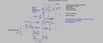
The resistor choices and output Z are completely illustrated in my Model at post 862.
http://www.diyaudio.com/forums/tubes-valves/183329-one-more-4p1l-se-18.html#post3986916
Re (intrinsic emitter resistance of BJT) increases with decreasing Ic.
You can estimate Re - it's the reciprocal of gm.
Gm = 40 * Ic (so 40mA/V at 1mA)
Re = 1/gm = 1/40 Kohm at 1mA
The resistor choices and output Z are completely illustrated in my Model at post 862.
http://www.diyaudio.com/forums/tubes-valves/183329-one-more-4p1l-se-18.html#post3986916
Hi Rod,
I may be a bit thick here. Not sure how you derived your Zo in your model? Looking at post 862, I estimated a gain of 14.5 when I plugged in the numbers and seemed about right looking at your simulation.
What puzzled me is when I simulate the driver in my circuit the gain plummets down to 2.5. I just changed the base resistor as suggested but I can't see how that may influence.
Is the feedback topology making that the reflected Rf different?
I can send post the LTspice asc file if needed
thanks
Ale
Attachments
One thing to check: the 4P1L models that are in-circulation are known to draw grid current.
How does the plot look, when Igrid1 is scoped?
Then again, it might just be that in pentode-mode, the anode voltage drops so fast that the driver gain is reduced.
Yes, please mail me the .asc, and I'll see if it can be restored to high gain.
How does the plot look, when Igrid1 is scoped?
Then again, it might just be that in pentode-mode, the anode voltage drops so fast that the driver gain is reduced.
Yes, please mail me the .asc, and I'll see if it can be restored to high gain.
No grid current. I developed the pentode model from real curves. It fits very well thanks to Derek's tool (Extract Model).
I will email you the files
thanks
Ale
I will email you the files
thanks
Ale
Hi Indra,
You're right, still can't explain gain difference with Rod's isolated driver simulation.
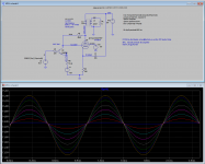
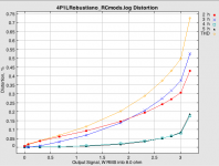
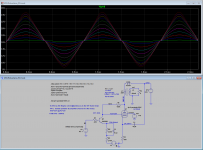
I played with it and got -3.5V and 2K for Re which seemed to provide good gain with a signal of just 2Vpeak for full output power. It seems good enough to try out this way. In practice I will tweak Rf to get the "sweet spot" on the harmonics and move a bit out of the pentode performance as shown in the THD attached. I ran briefly the FFT at 10kHz and distortion wasn't much greater. Perhaps this is the right circuit to try out?
I will build and report!!
You're right, still can't explain gain difference with Rod's isolated driver simulation.
I played with it and got -3.5V and 2K for Re which seemed to provide good gain with a signal of just 2Vpeak for full output power. It seems good enough to try out this way. In practice I will tweak Rf to get the "sweet spot" on the harmonics and move a bit out of the pentode performance as shown in the THD attached. I ran briefly the FFT at 10kHz and distortion wasn't much greater. Perhaps this is the right circuit to try out?
I will build and report!!
Attachments
Hi Ale,
Yes, It's the feedback action of the anode voltage that degenerates the gain.
Here it is with the fixes:
decoupler on the 4P1L cathode;
NPN emitter resistor partially generated only.
Now it easily achieves clipping, if desired.
Just mess with the relative values of RE & R3 to get the gain you need.
Yes, It's the feedback action of the anode voltage that degenerates the gain.
Here it is with the fixes:
decoupler on the 4P1L cathode;
NPN emitter resistor partially generated only.
Now it easily achieves clipping, if desired.
Just mess with the relative values of RE & R3 to get the gain you need.
Attachments
Hi Rod,
Thanks! We arrived close enough to same output THD from different sides. Your version is a tad more linear but we need to add the emitter bypass capacitor to partially degenerate the RE. I tweaked slightly the 4P1L operating point to bring it down to max Pa.
I also removed C2 as with C1 at 40-47uF should be enough to keep the -3dB below 10Hz. Actually if C1 is 30uF (ASC OIL cap) then the -3dB is 10Hz. I added primary leakage to look at HF roll off point. It is high, but haven't included the parasitic parallel R and C from the primary so should expect this to be different. Anyhow, it's good enough.
Distortion at 10kHz is only 0.55% at 3W (only 0.05% higher than at 1kHz). So this should be good then!
Case proven that the BJT driver is more linear than the FET one. I will build this version now to confirm the simulation results
Cheers
Ale
Attachments
- Home
- Amplifiers
- Tubes / Valves
- One more 4P1L SE