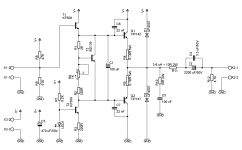
Hi guys, frankly could you tell me why the following scheme shoudn't work, maybe wrong resistor values or some common mistakes. .
.
It is supposed to come out as stereo hybrid amp with push-pull transistor output(~60W per channel) and 6N23P(E88CC) pre-stage.
Have a nice day, gentleman!
.It is supposed to come out as stereo hybrid amp with push-pull transistor output(~60W per channel) and 6N23P(E88CC) pre-stage.
An externally hosted image should be here but it was not working when we last tested it.
An externally hosted image should be here but it was not working when we last tested it.
Have a nice day, gentleman!
I don't know much about transistor circuits, but from my limited experience, there are five things that come to mind:
1. The coupling cap at the end of the tube stage (4.7uF) isn't particularly large. If connected to the next stage in the diagram, the corner frequency would be around 17Hz (not calculating the actual input impedance of the transistor itself, which would make matters worse), which is good enough, but I'm sure some people would prefer using a larger coupling cap.
2. I'm not sure about your power requirements, but it seems to me that the output stage is not necessarily the wisest solution. For one thing, it requires a fairly large 6800uF output coupling cap which, as far as I'm aware, would have to be rated for at least 115V (correct me if I'm wrong; I could very well be talking out of my behind here). Is this the best possible solution? Again, I don't know the first thing about transistor amps, but it seems that other topologies would be available that could circumvent this issue. I'm putting this remark here mostly to learn myself, not so much to provide feedback to your schematic.
3. I'm pretty sure you're going to pick up a lot of power supply hum in the tube stage with the limited filtering you're applying. It might be sufficient for the PP output stage, but I'd tap a HT line and apply extra filtering for the first amp stage to be sure. Have you simulated this power supply in any sort of software? I haven't, but it might give some useful results.
4. At first sight, the plate load of the input tube seems a bit small. I'm not familiar with this tube, but 6k8 doesn't look like much. It'll undoubtedly work, but I would like to hear the opinion of one of the more experienced gents here on this forum on this issue. I suppose there is a risk that instead of introducing a tube sound to the circuit, you might end up with some unwanted effects instead.
5. You'll have to tie the grid of the input tube to ground using a large resistor (say something in the range of 100k ~ 1Meg) in order to properly set the bias. If you don't do this, the circuit might work, but unpredictably.
So again, I'm posting the above primarily to create some discussion in order to learn myself a bit too. If you did consider these issues, I'd be interested to hear your opinion on them.
First thing I can see wrong is over an amp of bias current in the output stage bias string, almost all of which is going through the transistor base-emitter junctions. There are no emitter ballast resistors and the current design will saturate them. (If not melt them first) Collector current would be over 2A. There is no temperature compensation either.
You need a resistor to ground on the grid of your 6n23p. I have not checked to see whether or not the plate and cathode resistor values are reasonable.
The second stage is a phase splitter and the base should be biased ~0.7V above half of the supply voltage to provide symmetrical swing on the emitter and collector. You don't want any gain either and the emitter and collector resistors should be the same value.
What is the rated breakdown voltage of these transistors?
The power supply is also totally inadequately filtered.
As designed this circuit has no possibility of working. The solid state portion even with correctly selected component values is a very bad design, and should not be built as shown.
You need one high voltage supply for the tube, and a separate and much lower supply for the power amplifier stages.
Approximately +/-40V rails would be appropriate for an output stage designed to drive 8 ohm loads with 60W of output.
Last edited:
Would adding emitter resistors(same value as cathode resistors) solve this problem ? And what do you mean by "temperature compensation? Radiators ? Sorry, I'm quite new to thisFirst thing I can see wrong is over an amp of bias current in the output stage bias string, almost all of which is going through the transistor base-emitter junctions. There are no emitter ballast resistors and the current design will saturate them. (If not melt them first) Collector current would be over 2A. There is no temperature compensation either.

Cathode resistor value was on the tubes datasheet and I think plate resistor is the right value.I have not checked to see whether or not the plate and cathode resistor values are reasonable.
It actually is 115V, should I settle with supply voltage of 100V ?What is the rated breakdown voltage of these transistors?
How about I replace the choke, and add CRC filter in series ?The power supply is also totally inadequately filtered.
Would you direct me to some better designs?As designed this circuit has no possibility of working. The solid state portion even with correctly selected component values is a very bad design, and should not be built as shown.
Why so ? According to the datasheet the tube works fine at 100V. And why use lower voltage transistors ? If I use current ones, I don't have to add extra large power resistors to the power supply.You need one high voltage supply for the tube, and a separate and much lower supply for the power amplifier stages.
Yes, I think like 33uF would do better, but do I get cleaner signal at larger capacity or..?1. The coupling cap at the end of the tube stage (4.7uF) isn't particularly large.
Could you recommend some of better topologies ? If you think why I chose all transistors Ic to be min. 100V, it's because I didn't want to make power supply with like 20W resistors.2. I'm not sure about your power requirements, but it seems to me that the output stage is not necessarily the wisest solution. For one thing, it requires a fairly large 6800uF output coupling cap which, as far as I'm aware, would have to be rated for at least 115V (correct me if I'm wrong; I could very well be talking out of my behind here). Is this the best possible solution? Again, I don't know the first thing about transistor amps, but it seems that other topologies would be available that could circumvent this issue. I'm putting this remark here mostly to learn myself, not so much to provide feedback to your schematic.
I'm not sure I understand the term "HT line". To make power supply better, maybe I should use choke instead of resistor first and then put another CRC filter in series ?3. I'm pretty sure you're going to pick up a lot of power supply hum in the tube stage with the limited filtering you're applying. It might be sufficient for the PP output stage, but I'd tap a HT line and apply extra filtering for the first amp stage to be sure. Have you simulated this power supply in any sort of software? I haven't, but it might give some useful results.
Well I calculated it like this: Ra=100V/15mA. I think it's sufficient.4. At first sight, the plate load of the input tube seems a bit small.
Thanks, I'll do that.5. You'll have to tie the grid of the input tube to ground using a large resistor in order to properly set the bias.
You're going to get better low-end response, so more bass, put simply. But this isn't the biggest problem of your amp.Yes, I think like 33uF would do better, but do I get cleaner signal at larger capacity or..?
I don't have any experience with designing low impedance (transistor) amp circuits, so no, I couldn't suggest a better topology. Just picking a more or less random circuit from this message board, it seems to me that one of the advantages of transistors is that you don't necessarily need large output caps or transformers. See e.g. here: http://www.diyaudio.com/forums/solid-state/169590-mongrel-supersym-ii.html For me, that would be the primary reason to go for transistors instead of tubes.Could you recommend some of better topologies ? If you think why I chose all transistors Ic to be min. 100V, it's because I didn't want to make power supply with like 20W resistors.
HT = high tension, so a high voltage line. For a preamp tube stage I would personally use an extra RC filter and not bother finding a choke with high enough inductance. Of course, this will further drop the voltage, so you might have to change some values of the cathode and anode resistors on the input tube.I'm not sure I understand the term "HT line". To make power supply better, maybe I should use choke instead of resistor first and then put another CRC filter in series ?
I see, but in my understanding, a good rule of thumb is to choose the plate load at least 2x Ri (internal resistance) of the tube in case of a triode, in order to keep distortion low. Again, I'm not familiar with this tube, but I understand it has an Ri of something like 6k (correct me if I'm wrong!) I would therefore choose the plate resistor not smaller than 12k.Well I calculated it like this: Ra=100V/15mA. I think it's sufficient.
Also, biasing is largely a matter of taste, but running this tube in this particular instance at 15mA seems to me a bit odd. I'm not saying it can't be done, but in an application like this, I would expect it to be run at between 1 and 5mA. Then again, I might be talking out of my b-cheeks. Note that it also depends on how much voltage swing you need for the next stage. This should be the primary requirement around which you design the tube stage. Generally speaking, an entry stage will be of a relatively high impedance, hence my doubts about the small plate resistor and relatively high plate current. This is intuition speaking, not so much hard maths or objective reasoning, so perhaps some of the other members could chime in and give their thoughts on this as well.
Edit: actually, I am talking nonsense here. I see the tube you're using is equivalent to the ecc88, which has a low Ri. In that case, the plate load resistor is not _that_ odd, although most circuits I've come across (esp. preamp/gain stages) choose something upwards from 10k, and usually within the 30-60k range.
Last edited:
Member
Joined 2009
Paid Member
Wow. That is wrong everywhere. How powerful are you making the amp? If you use +-50v rails with 2-pairs of [good] output transistors you will get about 120-150 watts. No output cap needed for bipolar power.
A good place to start would be to get a good book on solid state amplifiers. The Doug Self and Bob Cordell books are good ones and current. Then hang around the solid state forum here, you will learn a lot.
THEN... tackle the hybrid.
Good luck,
..Todd
A good place to start would be to get a good book on solid state amplifiers. The Doug Self and Bob Cordell books are good ones and current. Then hang around the solid state forum here, you will learn a lot.
THEN... tackle the hybrid.
Good luck,
..Todd
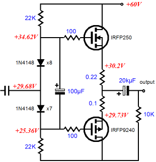
Tauri, give this output stage a try. You're using AC coupled output and a bunch of capacitors throught the amplifier as it is so the only difference is that this one is tested and works .. and it's dirt cheap
For desired output power adjust your supply voltage and key components (such as C2 and C3) accordongly depending your anticipated load (speaker impedance).
48V or so DC should get you into 30W into 8R output per channel power range so 60W total. Component values indicated here are for lower power.
T1 & T2 can be replaced with any medium power (few hundred miliwatts of dissipation) NPN types with decent beta (100 is good, anything more is even better because R8 & R9 can be increased to lessen the AC load on tube).
R11 is not just a resistor, it has 10-12 turns of roughly 1 mm diameter enamelled wire wound around it.
LED1 is the cheapest (= low brightness) red color kind.
Once powered up, tweak R6 until you get few tens of milivolts across R4 and R5.
Attachments
You misunderstood me, I suggested a lower power supply voltage of +/-40V for the output stage and not the tube, and I was not talking about the transistors themselves. Incidentally in a power stage such as this the power supply voltage should be appreciably less than half the rated VCE of the transistor to prevent breakdown when one transistor is close to saturation and the other is near cut off.Quote:
Originally Posted by kevinkr
You need one high voltage supply for the tube, and a separate and much lower supply for the power amplifier stages.
Why so ? According to the datasheet the tube works fine at 100V. And why use lower voltage transistors ? If I use current ones, I don't have to add extra large power resistors to the power supply, and only requires a single supply. Mount T3 on the heatsink with the power transistors and you will have some thermal compensation as I mentioned.
The output circuit posted by Arnulf should work well, and requires only a single supply. Mount T3 on the heatsink with the power transistors and you will have some thermal compensation as well.
You need to add lots of capacitance in the low voltage supply that should be present for the output stage. CRC filtering is not a good idea with the current required for a solid state output.
stage.. You should still use a high voltage supply for the tube stages, and a lower voltage supply for the output stage.
Last edited:
I can't say I follow this scheme allright.
1)What is the purpose of T1, T2 and T3 ? I mean, I see that signal is going to T1, and then to T2(wich in my eyes is the phase splitter)
Are they setting Q1 and Q2 biasing points ?
2)Why do we need LED1 and the diodes later(D1,D2)?
3)Also, I don't get it where Q2 gets its negative voltage? What is marked as GND is common wire what is connected to chassis of the amp. How can there be voltage ?
1)What is the purpose of T1, T2 and T3 ? I mean, I see that signal is going to T1, and then to T2(wich in my eyes is the phase splitter)
Are they setting Q1 and Q2 biasing points ?
2)Why do we need LED1 and the diodes later(D1,D2)?
3)Also, I don't get it where Q2 gets its negative voltage?
What is marked as GND is common wire what is connected to chassis of the amp. How can there be voltage ?I struggled with a "similar" topolgy with an aikido front end...this was the culprit - I had connected the zener bias network to the output or source of the MOSFETS. They hand voltage but would not bias up...I made PCB for the MOSFET stage and cut the trace that is in a similar position to the one I identified and voila!
I can't say I follow this scheme allright.
1)What is the purpose of T1, T2 and T3 ? I mean, I see that signal is going to T1, and then to T2(wich in my eyes is the phase splitter)
Are they setting Q1 and Q2 biasing points ?
2)Why do we need LED1 and the diodes later(D1,D2)?
3)Also, I don't get it where Q2 gets its negative voltage?
No negative voltage supply used. This design runs on a single positive supply.
T1 is an emitter follower provides high impedance load to the tube driving it. It also sets the dc voltage on the output stage to midpoint.
I recommend you get Morgan Jones "Valve Amplifiers, 3rd Edition" it will explain a lot of things including some basic stuff about semi-conductors. Fun read too.
T2 is a CCS providing a fixed high impedance load to T1 - this is good for linearity.. The LED provides a voltage reference to the base of T2.
The diodes D1 and D2 clamp the output so that back emf from the speaker cannot damage the output transistors.
T3 is a vbe multiplier which is used to set the quiescent operating current in the output stage. (Q1 and Q2) Mounted on the heatsink it will provide some thermal compensation by virtue of the transistor's negative vbe thermal voltage coefficient.
Incidentally this circuit is one of several RIGHT ways to do it - a good design.
I recommend Morgan Jones' "Valve Amplifiers, 3rd Edition" as it has a lot of useful information on audio design, including some basic stuff on semi-conductors. A fun read too.
Last edited:
You got that 2SC wired as a concertina splitter, and very asymetrical at that...
For your output stage, both + and - drives should have followed in same phase
with a voltage offset between them. Again, view Arnulf for practical example.
Arnulf circuit has no voltage gain of its own, so still needing triode up front.
For your output stage, both + and - drives should have followed in same phase
with a voltage offset between them. Again, view Arnulf for practical example.
Arnulf circuit has no voltage gain of its own, so still needing triode up front.
5. You'll have to tie the grid of the input tube to ground using a large resistor (say something in the range of 100k ~ 1Meg) in order to properly set the bias. If you don't do this, the circuit might work, but unpredictably.
I'm no expert, but doing this ('tie the grid of the input tube to ground'), then replacing 6k8 anode load resistor with constant current source, then using Arnulf posted output stage will surely work!!!
Arnulf circuit has no voltage gain of its own, so still needing triode up front.
Yes, this is the output buffer for tube front end, zero gain of its own. Its purpose was to eliminate OPT cost and shipping hassles from equation in order to encourage more people to delve into the wonderful world of tubes, it is a part of an article (a tube solid state hybrid).
Thanks to kevinkr for great explanation, I forgot to mention that T3 is supposed to be mounted on same heatsink as Q1 & Q2. I have it dead-center between both output darlingtons.
C3 is there just to take care of transients, PSU is on another PCB and has its own filtering capacitors which are significantly larger than C3 (2200 uF per ampere of anticipated peak current or larger) ! There simply is no room for larger capacitors on PCB for the buffer.
Perhaps I should also mention that this buffer fits onto a rather small (8x8 cm) single-sided PCB with zero jumper wires or vias so it can easily be etched and drilled at home.
Last edited:
- Status
- This old topic is closed. If you want to reopen this topic, contact a moderator using the "Report Post" button.
- Home
- Amplifiers
- Tubes / Valves
- 6N23P, transistor PP hybrid amp project.