Is this generic schematic of a long-tail pair phase splitter correct? Are there any additional parts (resistors or caps) that need to be added? I am using the schematic in a review. I drew it from looking at numerous variations on several websites.
John Johnson
John Johnson
Attachments
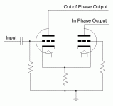
You are missing the plate load resistors, and perhaps output capacitors. You are also missing grid stoppers, and the input cap may be optional, depending on the presiding stage. And I almost forgot, where is B+? (called Vcc by the vulgar)
By the way, that is not a long tail pair. A Long tail pare would have a negative supply. Idea is that the cathode resistor is very large, to approximate a CSS.
HTH
Doug
By the way, that is not a long tail pair. A Long tail pare would have a negative supply. Idea is that the cathode resistor is very large, to approximate a CSS.
HTH
Doug
Last edited:
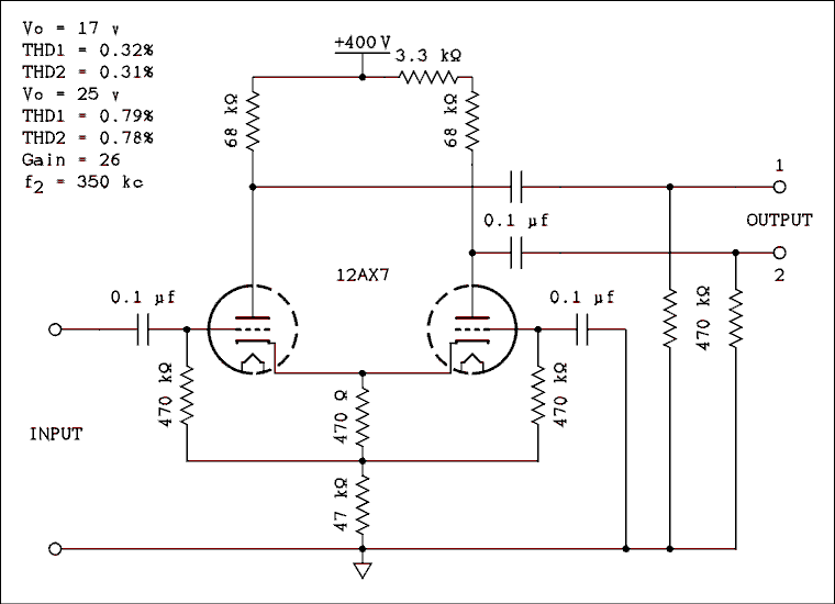
This is where I got most of the schematic for a long-tail pair phase splitter:
The Long-Tail Pair
Is his schematic incorrect, or did I just leave something out of my own schematic?
The Long-Tail Pair
Is his schematic incorrect, or did I just leave something out of my own schematic?
This is where I got most of the schematic for a long-tail pair phase splitter:
The Long-Tail Pair
Is his schematic incorrect, or did I just leave something out of my own schematic?
Requirements to values of long tail resistors and cathode bias resistors are very different. If you use in your schematic the value that is good for LTP tubes will be starving. If you use the value needed for proper bias it's no longer a LTP since the value of this resistor is too low for LTP.
Perhaps this one would be better to draw from (the schematic at the bottom of this URL):
http://www.angelfire.com/electronic/funwithtubes/Amp-Phase.html
http://www.angelfire.com/electronic/funwithtubes/Amp-Phase.html
If you want a LTP with very closely balanced signals then probably a small pentode as the current sink is best.
I am just about to try this but with a SV83. EF86 is described below.
Swap the 47K resistor for the pentode current sink.
I am just about to try this but with a SV83. EF86 is described below.
The ra of the pentode is so high compared to its cathode resistor that r(ccs) can be approximated as being equal to ra. In this case it is roughly 2Meg, so this circuit has the effect of using a 2Meg tail resistor on the long tailed pair, without the drawbacks! The performance of the long tailed pair becomes so perfect that its anode resistors can be made equal and excellent balance is ensured (see the sections on the long tailed pair for the rest of the circuit).
Swap the 47K resistor for the pentode current sink.
I will probably use the layout that aardvarkash10 illustrated
That's the common ltp layout but maybe you won't get the 2 signals very balanced. You may have to adjust the plate load resistors - 10% difference to balance the output.
The lower the tail resistor value the more unbalanced the output signals are.
That's why I'm going for the pentode sink instead of the 47K resistor.
Try this:
http://www.pentodepress.com/home/amplifier-calculators/long-tailed-pair/
I'm attempting an OTL hence the requirement for perfectly balanced phases.
Thanks much. I will probably use the layout that aardvarkash10 illustrated.
SY has done some interesting tests:
http://www.diyaudio.com/forums/tubes-valves/160312-balance-ccs-long-tailed-pairs.html
This might be helpfull for you:
http://homepage.mac.com/tlinespeaker...-CCS-beta3.pdf
regards
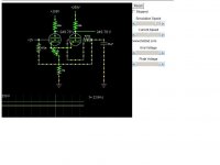
the below software is great as posted before.
http://www.falstad.com/circuit/e-mosfollower.html
I was playing around with it and you can create anything (only limitation is the type of triode), but it has CCS, resistors etc etc.
With this LTP below you can vary the tail resistor and see the effect on the output voltage. 1M will give you equal outputs (small pentode maybe), but 47K will not, but then you can try changing the plate resistor values until they match.
Really simple and fun. And you can save your work as a text file when you press export. Then import it after.
Attachments
Last edited:
the below software is great as posted before.
http://www.falstad.com/circuit/e-mosfollower.html
Nice pictures, but for an initial learning and understanding only.
It is greatly simplified. Especially, if to believe that MOSFET does not draw current, and it's output voltage is equal to input voltage minus some constant voltage. A first, current that mosfet draws is frequency dependent, and big enough relatively to DC resistance between gate and channel. It is the current that is needed to charge it's gate: it can't be charged immediately, so input resistance of MOSFET on AC is many times less than it's gate leakage resistance that people often assume as if it is MOSFET's input resistance. It may be represented by input, output, and gate to drain capacitances. This capacitances are non-linear, i.e. they are modulated by the signal.
Since current through mosfet is also modulated by the signal it's transconductance also is modulated by the signal, that means voltage drop can't be constant.
- Status
- This old topic is closed. If you want to reopen this topic, contact a moderator using the "Report Post" button.
- Home
- Amplifiers
- Tubes / Valves
- Long-tail pair phase splitter