Why fuss around with calculations? Build it and MEASURE! I very seldom caculate, but I do a LOT of measuring, and then I can be 100% certain.
Regards, Allen
Hi Allen,
Although I generally agree with that, I do think there is a place for calculation, (modeling, simulation...)
Sometimes I mess around with calculations to predict how a circuit will behave before building it, mainly to get the circuit closer to it's desired operation before building. It helps in deciding which parts and part values to select and sometimes rules out impractical circuit approaches.
It's also very instructive in cases like this to work through the calculation as a way to teach the circuit theory.
When a question like this comes up, it's an indication that the poster doesn't fully understand the operation of the circuit (otherwise he or she could easily construct the formula themselves).
It's also not clear in this case whether Joshua is building this or studying for learning purposes. In any case, building it is definitely the only way to be sure, but maybe not always necessary. Maybe if 3 circuits are analyzed, only one of them need be built.
So I think a good response would be to either teach the circuit theory through example or refer the poster to some reference material that teaches about cascode circuits.
There is enough of the circuit shown to teach the stage gain analysis. Several clues have been given.
Who can teach the analysis? Can Joshua now demonstrate how to estimate the gain of a cascode amplifier stage?
Hi Michael,
The question was not for studying purpose, I'm going to build a tape playback amp with the front end after Allen's phono stages, like in the schematic I posted (which is taken from Allen's website).
I admit I don't understand completely how cascoded stage work. Any explanation will be welcomed.
The question was not for studying purpose, I'm going to build a tape playback amp with the front end after Allen's phono stages, like in the schematic I posted (which is taken from Allen's website).
I admit I don't understand completely how cascoded stage work. Any explanation will be welcomed.
Why fuss around with calculations?
Because people often have limited time, and therfore can not afford to build on the off-chance that it might be right.
Because people often have limited money, and therfore can not afford to buy a stock of components just to experiment.
Because people often have limited time and money, and therfore can not afford to have circuits explode because they were designed wrong.
Because calculating is a proven professional way of taking a step towards a successful design. (And I don't just mean in audio, but in any technical subject).
Because calculating goes hand-in-hand with understanding, and understanding often leads to improved design, easier modification, easier fault-finding, and a good chance of success, and hence ultimately leads to a sense of intellectual reward.
If you want to do it the other way then best of luck to you, however I would encourage folks to understand and calculate before 'buying and trying'.
")
Why fuss around with calculations? Build it and MEASURE! I very seldom caculate, but I do a LOT of measuring, and then I can be 100% certain.
Regards, Allen
I guess nobody in this forum knows exactly how to calculate the gain or to analyze the circuit. People here normally judge a circuit by ear. Except me, of course.
I guess nobody in this forum knows exactly how to calculate the gain or to analyze the circuit.
You guess incorrectly. A = gm of the FET times the AC load resistance of the tube. The effective gm of the FET is modified by the source degeneration resistor.
I guess nobody in this forum knows exactly how to calculate the gain or to analyze the circuit. People here normally judge a circuit by ear. Except me, of course.
I'll give it try.
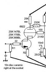
The JFET functions as a signal modulated current source. The scale of modulated current is determined by the effective transconductance, 'gm' (Amps per Volt) of the JFET stage, which includes the source resistor. This can be found by taking the datasheet transconductance figure, usually shown as milliamps per Volt, and converting milliamps per Volt in to Amps per Volt. Then, find the reciprocal value (1 / gm), then sum in the source resistor value (R2). Finally, find the reciprocal of this sum. The result will be the net effective transconductance of the JFET stage, in Amps per Volt.Since the JFET drain has a high impedance relative to the tube's cathode, the current conducted through that cathode is essentially contolled entirely by the JFET. Since the tube's cathode, anode (plate), and the anode (plate load) resistor are in series, the current conducted through the cathode will also be conducted through the plate load resistor, creating the output voltage.
Let's take an example, just for illustration. If the datasheet gm of the JFET were, let's say, 200mA per Volt and the source resistor (R2) were 20 ohms, the effective transconductance would be: (1 / 0.2A per Volt) + 20 ohms = 5 + 20 = 25, then 1 / 25 = 0.04A per Volt.
So, a 1 Volt input sgnal would produce a 0.04A current through the JFET drain. Which therefore means there would be a 0.04A current through the tube's plate load resistor. Now, we simply apply ohms law to determine the voltage amplitude across the plate resistor: 0.04A x 25kohms = 1,000 Volts! Of course, we don't need 1,000 volts, but it gives us the input to output voltage ratio (the gain) of the circuit for use with small signals. If 1 Volt in would give 1,000 Volts out, then the voltage gain is 1000x, which is 60dB.
Remember, this is just an first order calculation. I should expect that there might be second order effects that could somewhat reduce the calculated gain, which might be why Allen Wright (rest in peace) said to build the circuit and measure the actual gain.
Last edited:
I strongly agree with this post.Because people often have limited time, and therfore can not afford to build on the off-chance that it might be right.
Because people often have limited money, and therfore can not afford to buy a stock of components just to experiment.
Because people often have limited time and money, and therfore can not afford to have circuits explode because they were designed wrong.
Because calculating is a proven professional way of taking a step towards a successful design. (And I don't just mean in audio, but in any technical subject).
Because calculating goes hand-in-hand with understanding, and understanding often leads to improved design, easier modification, easier fault-finding, and a good chance of success, and hence ultimately leads to a sense of intellectual reward.
If you want to do it the other way then best of luck to you, however I would encourage folks to understand and calculate before 'buying and trying'.
Let's take an example, just for illustration. If the datasheet gm of the JFET were, let's say, 200mA per Volt...
100% agree, Ken. It should be noted that real FETs of the same nominal type are likely to have gms varying by 3:1 or more. Thus Allen's advice about building and measuring, unless you're willing to overbuy FETs and sort them to get the gm you want.
The gain of a cascode can be looked up in most good textbooks (which may be why there was reluctance to answer the question). The first order calculation has been given in this thread: gm x load. Second order corrections bring in the gm of the upper valve and the mu of the lower one, but these are small changes and can usually be ignored as they are within the usual range of spread of device characteristics.
My view is that if you can't at least estimate the gain, frequency response etc. of your circuit then you are not designing, merely throwing parts together. Simulation is a good way to check a design, but a poor way to do design. Measurement is a good way to check a design and should then lead to debugging: if gain is 30% lower than you expected then you may need to find out why.
My view is that if you can't at least estimate the gain, frequency response etc. of your circuit then you are not designing, merely throwing parts together. Simulation is a good way to check a design, but a poor way to do design. Measurement is a good way to check a design and should then lead to debugging: if gain is 30% lower than you expected then you may need to find out why.
A bit off topic, but could this FET-tube cascode be used as an output from a differential DAC? I have a RAKK DAC with outputs of .4V per leg with .4VDC on each leg. They usually use a couple of 91 ohm i/v resistors.
Active output
Active output
A bit off topic, but could this FET-tube cascode be used as an output from a differential DAC? I have a RAKK DAC with outputs of .4V per leg with .4VDC on each leg. They usually use a couple of 91 ohm i/v resistors.
Active output
Hi Andy,
I should think that jfet/tube cascode would have far too much gain. It believe it is intended as the input stage of a phono amplification chain. If you intend to take a differential output (both 'legs') from your DAC, then you will have a 0.8V output signal, which would require only 2.5x amplification to attain the ubiquitous 2V DAC output level. What is the full scale signal amplitude which you want to achieve?
Last edited:
It depends. If you have a current output DAC terminating in small resistors, a FET-tube cascode can work very well. If you have a voltage output DAC, the gain is likely to be too high (as Ken says) and there's not much advantage to using a complex circuit with low PSR.
edit: Looking at your link, that DAC has a current output which is meant to terminate into a virtual ground. I don't know if using 91R will degrade the performance- you might ask Dave Davenport directly, he's a very sharp guy. If the 91R is OK, you need very little gain out of the following stages, maybe between 0 and 6 dB; it merely needs buffering. Cascode is not the first choice for that.
edit: Looking at your link, that DAC has a current output which is meant to terminate into a virtual ground. I don't know if using 91R will degrade the performance- you might ask Dave Davenport directly, he's a very sharp guy. If the 91R is OK, you need very little gain out of the following stages, maybe between 0 and 6 dB; it merely needs buffering. Cascode is not the first choice for that.
SY,
I believe the RAKK DAC utilizes the PCM1794A, which is one of the few current output DACs which performs well while developing an substantial A.C. voltage on it's output pins - meaning, with passive resistor I/V. My own experimental DAC design utilizes this chip with 150 ohm passive I/V resistors, wherein THD measures around 0.002% @ -3dBFS via my 24-bit soundcard and FFT audio analyzer software.
I believe that several commercial digital source vendors, such as Audio Research and Ayre, utilize the PCM1794A with passive resistor I/V values of up to 200 ohms. Passive resistor I/V has been subjectively far more transparent sounding than the op-amp based transimpedance converter I had once used.
Last edited:
If that's the case, a simple buffer ought to do fine. If one wants pro levels, 6dB of gain will get you there.
I've A.C. coupled a single phase of my DAC output to my JFET line-stage with no intervening active circuitry. The 400mVRMS DAC output is plenty, given the 20dB gain of the line-stage.
How do you work the anti-imaging filter?
I use a first order passive filter, a 100pF NP0 ceramic SMD across the PCM1794A's differential current outputs, as near as I can get to the chip's pins. I've not yet experimented with multi-pole passive filters, as they would require utilizing either inductors or cascaded lossy RC stages. But who knows, my DAC's output spectra may be provoking audible IMD products in my line-stage or power amp, which would be reduced with a higher order filter. Another experiment to add to the list I suppose.
Last edited:
- Status
- This old topic is closed. If you want to reopen this topic, contact a moderator using the "Report Post" button.
- Home
- Amplifiers
- Tubes / Valves
- JFET cascoded with tube gain calculation