Hi,
The basic idea comes from smoking-amp in another thread:
http://www.diyaudio.com/forums/tubes-valves/160240-suppresor-grid-used-feedback-10.html#post2098113
The linearity is similar to screen drive but the voltage swing required is much less.
I adapted an amp design I've been developing to try out the concept. I haven't built it yet; still in the conceptual phase.
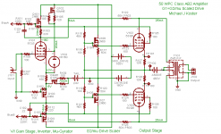
The basic topology is class AB, local current feedback loading a pentode+MOSFET CCS LTP gainstage and inverter with gyrators in the anode supply. Current feedback is derived across R122 and R125
The screen drive method borrows from some class A2 amps I've built, using the "mu output" of the gyrator for super-low drive impedance.
The scaled G1 drive voltage is generated by voltage divider R115, R116 from G2 to cathode. This is then buffered by MOSFET source follower Q106. There will be about 5V offset G2 positive WRT G1 in addition to the scaling this way (not sure of the effect...)
I show a stacked power supply arrangement with a third grid drive supply returned to the output cathodes. This keeps the grid current local to the output tube loop from grids to cathode. Other arrangements are certainly possible but I have had good results with this.
I guess the 6DQ6 gm to be around 3500-4000 wrt G2 using scaled drive, resulting in an effective anode resistance of 250-300 ohms in this circuit, hence the 6K6 OPT Zpri giving a damping factor of say (300+DCR) /1650 or about 5.
I think the sensitivity is about 2VRMS input for full sinewave output of about 50W. That can be tweaked by replacing all or part of R108 with diodes.
Comments or suggestions are welcome!
Michael
The basic idea comes from smoking-amp in another thread:
http://www.diyaudio.com/forums/tubes-valves/160240-suppresor-grid-used-feedback-10.html#post2098113
The linearity is similar to screen drive but the voltage swing required is much less.
I adapted an amp design I've been developing to try out the concept. I haven't built it yet; still in the conceptual phase.
The basic topology is class AB, local current feedback loading a pentode+MOSFET CCS LTP gainstage and inverter with gyrators in the anode supply. Current feedback is derived across R122 and R125
The screen drive method borrows from some class A2 amps I've built, using the "mu output" of the gyrator for super-low drive impedance.
The scaled G1 drive voltage is generated by voltage divider R115, R116 from G2 to cathode. This is then buffered by MOSFET source follower Q106. There will be about 5V offset G2 positive WRT G1 in addition to the scaling this way (not sure of the effect...)
I show a stacked power supply arrangement with a third grid drive supply returned to the output cathodes. This keeps the grid current local to the output tube loop from grids to cathode. Other arrangements are certainly possible but I have had good results with this.
I guess the 6DQ6 gm to be around 3500-4000 wrt G2 using scaled drive, resulting in an effective anode resistance of 250-300 ohms in this circuit, hence the 6K6 OPT Zpri giving a damping factor of say (300+DCR) /1650 or about 5.
I think the sensitivity is about 2VRMS input for full sinewave output of about 50W. That can be tweaked by replacing all or part of R108 with diodes.
Comments or suggestions are welcome!
Michael
Attachments
Michael,
Interesting design. I see some anti-triode driver snuck in there too.
I did some further measurements for the 6HJ5 on the curve tracer using the resistor divider scaled drives. I found that the g2 was ramping up to 5 mA while the g1 was ramping up to 20 mA, with stepping from 0 to 55 V on g2 (1/4 that on g1). There was just a small amount of upward curvature in the current ramps versus voltage steps, probably the beginning of a diode curve (and a current spike around 0 V plate voltage). Would really need about twice that voltage range to fully test I think, but so far it looks as if the two grid inputs have near-enough resistive characteristics. So I am planning on just using a resistive divider from the g2 Mosfet follower drive down to the g1 for my first proto test ( g1 impedance is even conveniently scaled for the divider). A little droop in the g1/g2 ratio might actually further linearize the transfer anyway.
Probably can't use the simulator models for the output stage? At least I wouldn't expect the grid currents to be well modeled. But some scaled diode V to I may work for those.
For my 1st proto I'm thinking of using two 5 Watt video pentodes for drivers, with Schading feedbacks from the output plates to the driver cathodes. Since that ups the driver grid input voltage requirements, I will use some triodes (freebies in the video bottles) to make an LTP splitter up front.
Last edited:
I'm thinking of approaching the scaled drive concept from another viewpoint, but it will require a custom transformer. One comment - the control grid gets a follower, but the screen doesn't. You might consider running the follower into the screen instead, with a resistive divider to the control grids. I would think that being farther up on the drive feeding chain, the screens are more likely to pull current and require the services of a follower.
On the 6HJ5 (triode Mu 4.2) I found that the g1 draws 4X the current of the g2 grid (using 1/4 the voltage drive of g2). Probably some shielding of g2 occuring with the aligned grids, but one would also expect a positive g1 to "focus" electrons on g2 at some point. Maybe there will be some nasty "phase change" at a higher drive voltage than the +55V I have tested (on g2) so far.
I'm hoping that positive g1 causes the focusing focus point to occur short of the g2 wires, causing a crossover spray of electrons that largely misses g2. Have to get the proto together to find out. Certainly, g2 will take the brunt of the current when the plate V drops below 50 V (observed on the tracer, biggest current spikes on g2 at low plate V. Hmm, I'm going to re-check that again, not real sure). Would be nice if g2 could droop a bit under that abuse.
Michael does have the Mu follower to drive the g2.
Last edited:
I have been working on a circuit to drive both grids at once for a while. I have performed a few experiments along these lines and none resulted in anything useful. That hasn't stopped the process though, and if it rains tomorrow the switch might get thrown on my biggest step in this direction yet.
Years ago I found mention of a "high Mu triode" connection in the data sheet for a medium sized pentode (or tetrode) DH transmitting tube. It simply had G1 and G2 tied together. If my memory isn't faulty (highly possible) there were curves for this mode. I can not find that info anywhere now, but I have changed computers several times since then, and it might have been on paper.
At about the same time I saw a circuit for an amplifier using a pentode (807 I think) where G2 was directly driven and there was a resistor from G2 to G1. It was a push pull design using an interstage transformer. I breadboarded something similar using 6L6GC's and remember a whole bunch of power and a whole bunch of distortion. It sounded like some of my early amp experiments using the big germanium power transistors salvaged from 1960's car radios.
More recently (the Tube Sale at AES thread) I was melting tubes in screen drive mode (over 100 watts from a pair of 98 cent 6BQ6's) when I got the idea to tie G1 to G2 and drive them both with a PowerDrive circuit. The whole thing went bang on power up and there wasn't much left of the mosfets. I chalked the failure up to a wiring error (an unproven guess).
About a week later after some more successful other experiments I returned to the G1=G2 connection only to have it blow up again. This time I know it was wired right, so maybe oscillation was to blame. I gave up on this idea.
After reading the above mentioned thread and looking at the 6HJ5 curves I have decided to try it again. This time I am not going to tie the two grids together. I know that a mosfet buffer works to drive either G1 or G2 (done that on numerous tubes) and I know that a 6SN7 can drive two mosfets to the 200 V P-P level (done that to drive multiple tubes) so why can't I drive 2 mosfets from one 6SN7 and wire one mosfet to each grid of a power tube?
Since I tried some similar experiments back in the Adjustable Distributed Load thread, but never finished my experiments, these ideas should be investigated too. In fact it was the discovery of the breadboard for those experiments while closet cleaning that prompted this "lets blow it up one more time before tossing it" round of experiments.
Well I haven't done much thinking about it yet, but I do have hardware. In this case it is an ugly sky wired breadboard that never worked being given one more chance at life. I know that one or more mosfets are blown (there is a crater in the plastic) so I need to replace them all (4). I plan to wire this up to my octal driver since it works good. Output tubes? Something octal, cheap, and plentiful (not 6HJ5), maybe 6BQ6's, 6L6GC's or 6AV5's.
I have several "HoneyDo" projects lined up for tomorrow, but they are all outdoors. Lets hope it rains, it rained most of today.
Years ago I found mention of a "high Mu triode" connection in the data sheet for a medium sized pentode (or tetrode) DH transmitting tube. It simply had G1 and G2 tied together. If my memory isn't faulty (highly possible) there were curves for this mode. I can not find that info anywhere now, but I have changed computers several times since then, and it might have been on paper.
At about the same time I saw a circuit for an amplifier using a pentode (807 I think) where G2 was directly driven and there was a resistor from G2 to G1. It was a push pull design using an interstage transformer. I breadboarded something similar using 6L6GC's and remember a whole bunch of power and a whole bunch of distortion. It sounded like some of my early amp experiments using the big germanium power transistors salvaged from 1960's car radios.
More recently (the Tube Sale at AES thread) I was melting tubes in screen drive mode (over 100 watts from a pair of 98 cent 6BQ6's) when I got the idea to tie G1 to G2 and drive them both with a PowerDrive circuit. The whole thing went bang on power up and there wasn't much left of the mosfets. I chalked the failure up to a wiring error (an unproven guess).
About a week later after some more successful other experiments I returned to the G1=G2 connection only to have it blow up again. This time I know it was wired right, so maybe oscillation was to blame. I gave up on this idea.
After reading the above mentioned thread and looking at the 6HJ5 curves I have decided to try it again. This time I am not going to tie the two grids together. I know that a mosfet buffer works to drive either G1 or G2 (done that on numerous tubes) and I know that a 6SN7 can drive two mosfets to the 200 V P-P level (done that to drive multiple tubes) so why can't I drive 2 mosfets from one 6SN7 and wire one mosfet to each grid of a power tube?
Since I tried some similar experiments back in the Adjustable Distributed Load thread, but never finished my experiments, these ideas should be investigated too. In fact it was the discovery of the breadboard for those experiments while closet cleaning that prompted this "lets blow it up one more time before tossing it" round of experiments.
I adapted an amp design I've been developing to try out the concept. I haven't built it yet; still in the conceptual phase.
Well I haven't done much thinking about it yet, but I do have hardware. In this case it is an ugly sky wired breadboard that never worked being given one more chance at life. I know that one or more mosfets are blown (there is a crater in the plastic) so I need to replace them all (4). I plan to wire this up to my octal driver since it works good. Output tubes? Something octal, cheap, and plentiful (not 6HJ5), maybe 6BQ6's, 6L6GC's or 6AV5's.
I have several "HoneyDo" projects lined up for tomorrow, but they are all outdoors. Lets hope it rains, it rained most of today.
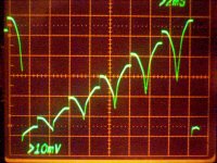
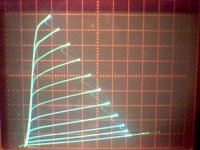
Here are some pics. These were taken on a timebase scope rather than the curve tracer, so are versus time rather than plate voltage as on the tracer. 11 stepped traces are sequenced, with every other one using an opposite 90 degree side of the power line sine wave voltage. There are actually two slightly different versions, since 11 does not divide out evenly by twos (rising and falling edges of 60 Hz may be reversed between sets) so some miss-match may be present between pics since 60 Hz sync was unknown on the scope. But general trend is obvious. ( I need to get the curve tracer set up to accept an external vertical signal so I can do regular grid current curves)
Current signals here was from a Tek AM503 DC current probe setup. Grid drives were 4 to 1. +55V max stepping on g2.
1) cathode current 50mA/div
2) plate current 50 mA/div
3) g1 current 10 mA/div
4) g2 current 10 mA/div
I'm puzzled by the cathode current and plate current traces, should be more similar I would think. Maybe I got the scale wrong on one. Well, at least one can see that the g2 current is the most spikey when plate voltage is low. Looks like g2 baseline current ramping is about half the g1 current ramp. Close to linear current ramps overall for g1 and g2, but some curvature upwards, probably a diode V/I curve. g2 looks more curved. g1 being closer to a straight ramp (resistive Z) is desirable as far as using just one Mosfet driver with a resistive divider for g1.
Attachments
Last edited:
The resistive divider in the previous pics was approx. 300 Ohm from g2 to g1 and 100 Ohm from g1 to cathode. The 300 Ohm was adjusted until the voltages on the grids were 4 to 1. With 55V max stepping, that would be 137 mA thru the divider alone. But g1 is drawing about 80 mA max. Not a problem if it is a linear Z, since the attenuator was adjusted for a 4 to 1 result, but since it is not strictly linear, it may be causing the straigtening of the g1 current curve, since it would reduce the divider ratio as it draws excess (above the expected linear ramp) current. Probably g1 is just as curved as g2. I'll have to rig up a Mosfet g1 driver to test it on the tracer again.
Hmmm, maybe it will eventually be useful to put some extra resistance in the g2 leg too. The non-linear current draw by the grids is self linearizing that way (versus the internal 3/2 power transfer function).
Hmmm, maybe it will eventually be useful to put some extra resistance in the g2 leg too. The non-linear current draw by the grids is self linearizing that way (versus the internal 3/2 power transfer function).
Last edited:
S/A -
In retrospect, what you found makes sense, as the control grid is closer to the cathode than the screen, so it should draw more current for a given positive drive. The place to look for freaky behavior will be at screen voltages of about 100V or so, though with the scaled G1/G2 drive 50V is as likely to drive the tube as hard as 100V G2 drive alone. I'd expect to only see such excursions at or near clipping for sufficiently frisky drivers.
In retrospect, what you found makes sense, as the control grid is closer to the cathode than the screen, so it should draw more current for a given positive drive. The place to look for freaky behavior will be at screen voltages of about 100V or so, though with the scaled G1/G2 drive 50V is as likely to drive the tube as hard as 100V G2 drive alone. I'd expect to only see such excursions at or near clipping for sufficiently frisky drivers.
Here are some pics. These were taken on a timebase scope rather than the curve tracer, so are versus time rather than plate voltage as on the tracer.
(...)
1) cathode current 50mA/div
2) plate current 50 mA/div
3) g1 current 10 mA/div
4) g2 current 10 mA/div
I'm puzzled by the cathode current and plate current traces, should be more similar I would think. Maybe I got the scale wrong on one. Well, at least one can see that the g2 current is the most spikey when plate voltage is low. Looks like g2 baseline current ramping is about half the g1 current ramp. Close to linear current ramps overall for g1 and g2, but some curvature upwards, probably a diode V/I curve. g2 looks more curved. g1 being closer to a straight ramp (resistive Z) is desirable as far as using just one Mosfet driver with a resistive divider for g1.
Thanks all for the comments!
It looks to me like the cathode current is close to the expected sum of all other electrode currents. Peak g1 and peak g2 current are on the same order of magnitude as each other, but G1 seems more linear resistive and g2 acts more like a diode as plate voltage goes lower.
I'm not too worried about the G1 current, but the allowed G1 dissipation is not specified for sweep tubes. I am assuming it's good for at least one watt. The current would need to be >200mA at +20V peak to dissipate anywhere near 1 watt.
I think some trial and error is going to be needed; I will do a lot of in-circuit test and measurement. I will stick with the g1 follower for now so I can easily experiment with varying the DC bias offset on g1.
@kenpeter: I think 40K/10K will drive the Crss of the scaler follower OK. Aren't the Ciss and Coss bootstrapped in this circuit? However there's not a problem lowering the impedance of the divider down below 1K if needed e.g. to drive G1 directly. The mu-gyrators may need a bigger heatsink though...
@wrenchone: If this drive method needs more than 100V peak, the gm will be too low for the local feedback topology in my application. I don't think tubes with low pentode gm (6L6 types) or higher mu (EL34, 6550) will work as well as sweep tubes in this circuit, but 6l6s and 6550s work well enough as pentodes with G2 at B+ anyway.
@George: This does seem to be very little different from the "high impedance triode" mode of operation you describe. This same circuit without the extra g1 scaler/follower will drive high impedance triodes and give low effective output resistance.
@Anatoliy: I have never understood the popularity of ultralinear. By the time you add enough NFB to get a decent output resistance you can consider a number of other options like local Schade feedback *instead*. I suppose I need to read H&K again ... or not ;-)
Cheers,
Michael
Last edited:
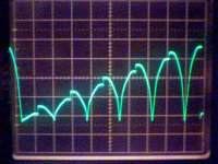
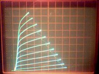
Here is a plot of actual g2 and g1 voltages using just the resistive divider to drive g1. I adjusted the divider to get twice the current level of plate curves with g1 and g2 versus g2 only. Then I checked the divider resistance, and its running at 268 Ohm from g2 to g1 and 100 Ohm from g1 to cathode. Tube Mu is nominally 4.2. So would expect 300 Ohm and 100 Ohm if g1 weren't drawing current. Can see from the plot that g1 voltage is drooping at higher stepping levels. I adjusted the attenuator on the scope to get matched 1st step levels between them. Or put a ruler to the g1 steps and see the droop.
Scale on the g2 curve is 5 V per div. according to the scope (but 5.3 V steps according to the curve tracer, someones calibration?), g1 curve should be about 1/4.2 of that, the variable attenuator was used on g1 to get a match.
I just checked the tracer step output using a DVM and get 3 V steps. Looks like the scope is right. Which means I've only been getting 30 V max for 10 steps.
Ugh, just found the problem, the variable step gain control on the tracer wasn't at its max setting.
I'm going to set up a Mosfet follower for g1 next.
Attachments
Last edited:
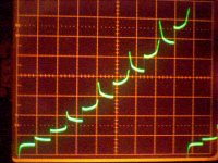
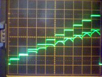
Re-did the g2 and g1 voltage plot for 6HJ5 with the max step setting of 5.3 V steps per the tracer (6V steps per the DVM, and about 5.9 V steps according to the scope). Vertical scale here is 10 V per div. (scope) for g2. This is using the same resistive divider for g1 again.
The jaggies in the g1 curves on each step are from when plate voltage is near zero (occurs on leading or falling edge depending on the phase of the 60 Hz plate voltage).
Clearly, g1 voltages are drooping off with high g1 current and/or low plate voltage, when just using a resistive divider.
OK, on to getting a Mosfet driver set up for g1 finally.
Attachments
Last edited:
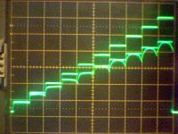
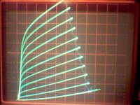
Here is Mu scaled g2,g1 6HJ5 with a Mosfet driver for g1 now. 50 mA/div vert. and 50 V/div horiz. 5.3 V steps on g2. Approx 4/1 scaling. The divider is still between g2 and cathode here, but g1 is buffered by a Mosfet follower (which has a few volt gate threshold unfortunately)
2nd plot is the earlier resistive divider curves. Same setup except no Mosfet driver.
Looks like the Mosfet driven g1 curve set is more squared up (no more g1 sag at low plate V). The lower bunched together plate curves are due to the Mosfet turning off below its gate threshold, so only g2 drive there. I'll have to rig up some DC biasing for the g1/Mosfet next, to fix the gate threshold problem.
Attachments
Last edited:
I have never understood the popularity of ultralinear. By the time you add enough NFB to get a decent output resistance you can consider a number of other options
I try to keep an open mind toward most things involving audio and electronics. 5 or 6 years ago when I was advocating the use of a mosfet follower for grid drive the response from the tube audiophile community was overwhelmingly negative. No look how far we have come.
I don't have a strong opinion on UL but I have found applications where it works well. Consider my Simple SE design. It is a simple circuit using a CCS loaded triode (half a 12AT7) driving a pentode (EL34, 6L6GC or KT88). The output stage can be connected in triode, UL, or pentode via jumpers or a switch. Local cathode feedback can be enabled via a jumper or a switch. 90% of the time I have the amp in triode mode without feedback using KT88's. There are times however where UL with cathode feedback just sounds better. These times usually involve music like Pink Floyd or Depeche Mode. Other Simple SE users have come to similar conclusions.
This does seem to be very little different from the "high impedance triode" mode of operation you describe.
I like the curves you post better than the typical high Mu beam triodes like the 6HV5. Unfortunately I didn't get to experiment this weekend. Instead I spent the weekend outside making my yard look better than the empty forclosures on the block. The weather radar has been green, yellow, and red all around us, but I only got wet once today.
Even though I was outside working for most of the weekend, by brain kept dreaming up circuits. For now my plan will be to use a pentode from the dollar menu as a driver / splitter. Multiple mosfet buffers will feed each grid. Schade style feedback will be used. Dollar menu sweep tubes and high Mu beam triodes are the initial "test subjects".
Here is the scaled g2,g1 6HJ5 using Mosfet drive on g1, with DC biasing to fix up the Mosfet gate threshold.
I ran into a problem here though using a cap to couple divided down g2 signal to the Mosfet gate. A protection zener diode across the Mosfet gate to source conducts when the drive signal is large enough, changing the charge on the cap (a blocking problem). I have a 2.7K Ohm resistor loading the Mosfet source to 0 V at the cathode, which provides the conduction path when AC drives it below 0 V. I was able to adjust the bias upwards (half of AC signal approx.) to get things to work, but if I change the # of steps on the curve tracer, I have to re-adjust the DC bias every time. Not good for real signals.
SOooo, either I have to return the Mosfet loading resistor to a negative (more than -1/2 max peak drive AC on g1) voltage to avoid blocking, or go with some type of DC coupling offseted to fix the Mosfet gate threshold.
Another problem also came up too. I had to operate with reduced g1 AC (1/6 of g2 AC here for the plot shown) in order to avoid some kind of saturation problem of the tube plate current. (I had plenty, 36V, of g1 Mosfet drain voltage to avoid saturation there) The top curves start bunching together (at the low plate voltage end of the curves) if I increase g1 drive beyond 1/6 of g2. Not sure what the problem is yet. Maybe g2 starts eating the plate current too much? More testing in order.
Attachments
edit (late):
The bunching effect at high plate currents may just be a visual artifact due to the curve tracer load limiting resistor not allowing/showing more than the low plate voltage part of the curves there. I also couldn't see any particular pick up in screen currents there either with the divider cranked up and a current probe. When I switched to a 140 Ohm load resistor (220 Watt limit) on the tracer from the usual 650 Ohm (50 Watt limit), the bunching effect disappeared. (The cardboard the tube was sitting on started smoking though!) More testing in order.
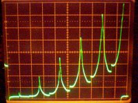
HeHe:
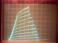
6HJ5 at 220 Watt peak limiting plot attached, scaled g2g1 drive. 100 mA/div vertical. Note that the increased g1 drive here is causing the knees of the plate curves move to higher plate voltages than before. The g2,g1 divider was at 82 Ohms from g2 to g1 pickoff, and 100 Ohms from there to ground.
The bunching effect at high plate currents may just be a visual artifact due to the curve tracer load limiting resistor not allowing/showing more than the low plate voltage part of the curves there. I also couldn't see any particular pick up in screen currents there either with the divider cranked up and a current probe. When I switched to a 140 Ohm load resistor (220 Watt limit) on the tracer from the usual 650 Ohm (50 Watt limit), the bunching effect disappeared. (The cardboard the tube was sitting on started smoking though!) More testing in order.
HeHe:
6HJ5 at 220 Watt peak limiting plot attached, scaled g2g1 drive. 100 mA/div vertical. Note that the increased g1 drive here is causing the knees of the plate curves move to higher plate voltages than before. The g2,g1 divider was at 82 Ohms from g2 to g1 pickoff, and 100 Ohms from there to ground.
Attachments
Last edited:
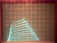
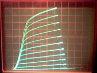
Since Michael is using 6DQ6 outputs, I dug out some 12GE5s which are essentially the same tube as 6DQ6B or 6JN6A. This tube has a Mu of 4.4, 17.5 Watt diss. rating.
1st plot is operating in scaled g2,g1 mode with the Mu divider at 4.4 and using a Mosfet driver with gate biasing. Scale is 50 V/div horiz. and 50 mA/div vert. 5.3 V/div stepping. (usual 50 Watt peak load limiting on the tracer)
2nd plot is with 220 Watt peak load limiting on the tracer (140 Ohm load resistor), same vert and horiz scales, same 5.3 V steps and Mosfet g1 driver. Mu divider was 79 Ohms from g2 to g1 pickoff and 100 Ohms from there to cathode.
Hey, you ought to be able to get 400 Watts out of these in P-P for a few seconds at least.
Attachments
Last edited:
Hey, you ought to be able to get 400 Watts out of these in P-P for a few seconds at least.
That sounds like a challenge to me. Well I got two $1 tubes wired together as a phase splitter. With 2 volts into the stage, I get two out of phase signals at about 350 V P-P. Buffer that with mosfets and I should be able to melt any grid ever made! I may have some ugly looking old 6DQ6's somewhere.
- Status
- This old topic is closed. If you want to reopen this topic, contact a moderator using the "Report Post" button.
- Home
- Amplifiers
- Tubes / Valves
- G1=G2/mu Scaled Drive Strawman Design