What explanation had been provided for that claim?
The guy who presented his data believed that the partition noise was eliminated because both plate and screen current went through the plate load resistor. I have not confirmed his data, just putting up his circuit as an interesting alternate approach.
I don't have a copy of his presentation, but if memory serves, the series screen resistor was a stopper, maybe 1k, and the series string was chosen to have one or two orders of magnitude more current than the transistor base.
")
One issue with the screen current bypass/re-combiner scheme is that the resultant tube curves look nothing like what they did before. Forget about it sounding the same.
The rounded knees that pentodes typically have become square, just like a Mosfet. (not the fault of the bypass device though) Normal screen current loss is the cause of the rounded knees. Put it back, and its back to square. More 2nd harmonic shows up then, sharper clipping. I've run the Mosfet/tube-pentode setup on a curve tracer, and the worst looking pentode curves you can find square right up into the cleanest Mosfet like curves. You might just as well use a Mosfet for the whole thing in the first place.
The rounded knees that pentodes typically have become square, just like a Mosfet. (not the fault of the bypass device though) Normal screen current loss is the cause of the rounded knees. Put it back, and its back to square. More 2nd harmonic shows up then, sharper clipping. I've run the Mosfet/tube-pentode setup on a curve tracer, and the worst looking pentode curves you can find square right up into the cleanest Mosfet like curves. You might just as well use a Mosfet for the whole thing in the first place.
Last edited:
leadbelly, how does questioning about small signal and clipping irrelevant when the opening is:
" Lowering noise in small signal pentodes?
So, I have been searching and reading up on the various sources on how to apply small signal pentodes to input stages, and more specifically, how best to treat g2"
Constitute a strike and attempt to hijack the thread? I am questioning why large signal distortion is an issue when we are talking about using pentodes for small signal amplification.
leadbelly, how does questioning about small signal and clipping irrelevant when the opening is:
" Lowering noise in small signal pentodes?
So, I have been searching and reading up on the various sources on how to apply small signal pentodes to input stages, and more specifically, how best to treat g2"
Constitute a strike and attempt to hijack the thread? I am questioning why large signal distortion is an issue when we are talking about using pentodes for small signal amplification.
1) How exactly does one hijack their own thread?
2) Who said ANYTHING about clipping or large signal distortion? I certainly didn't.
EDIT: Oops, my apologies, you were replying to smoking-amp about clipping...I didn't see that.
Last edited:
Apology accepted, no foul.
So back to my question, does clipping mater in this case where we are talking about using pentodes as small signal amplifiers?
Say we are doing a phono input stage, and we are amplifying 4.4mV rms with a gain of 100 (maybe not realistic). We have a supply of 200V and we are biased with the anode at 100V. The largest signal excursion will be 4.4 * 1.414 * *2 * 100 = 1.24Vp-p.
With less than 2v p-p swing we shouldn't have to worry about clipping, and should be able to restrict our operation to a fairly linear region. If partition noise IS addressed by the discussed circuits (and I'm not sure yet), then what are the remaining issues?
Ignoring partition noise are there other noise factors of small signal pentodes that would be of concern?
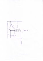
Sorry for the hand drawing.
I use this circuit in the g2 supply of a 13E1 Se.I was recommended this circuit by 7N7, who used it in the g2 supply of a pentode cathodefollower.
Initially I had S130P (pre ww2 vr tube) but it was not performing as well as the other vr tubes in the amplifier( driver tube is pentode with 0c3 in g2 supply, unbypassed cathoderesistor).
The amplifier delivers 32-34 w .
THD 1,2 % at onset of clipping.noise on output with 1 k termination on input, is 400µv.with the 400 hz filter connected around 100µV.
As a newbie many things is unclear.can anyone explain if the cap from collector to ground is needed when b+ is regulated ?
Vega,
Coming in a little late ..... that cap has nothing to do with B+ regulation. In your sketch the collector (I presume the lead going to screen is the emitter) has signal on it coming from the OPT; the capacitor is to bypass that.
As your drawing stands, it rather looks like a UL type arrangement for a screen at lower voltage for a power amplifier. I cannot quite read the value of the emitter capacitor. Is this circuit supposed to have something to do with lowering noise?
I once significantly reduced noise powering 6J32P filament from 5V voltage regulator.
A lower cathode temperature can give lower noise, especially in small-signal cases. In a manner of speaking, decreasing the electrons 'rushing past' while they are not used (needed), lowers their 'noise effect.' I have done this occasionally, but never tried to optimise. It could well be that such an effect might be sensitive to cathode temperature, which might mean some heater voltage stabilization might be needed. But then in all probability there will be dc on heaters as the subject would only be of concern at low signals - in which case stabilization is possible. (ICs are cheaper than big electrolytics, so make good ripple eliminators in addition to regulating.)
Not sure whether already mentioned (I did not peruse all posts), but did anyone experiment with value of screen voltage? Gain goes down with screen voltage, but is this linear?
First my apologies to threadstarter. It was not my purpose to post of topic.I was in a hurry and did not present my thoughts clear enough.
You ask how to best treat g2.
The circuit shown is not mine .I got it from Paul Leclerc (7N7 at forum)
He has been kind enough to give me some advise as I have progressed in making a 13E1 Se amplifier.
First i tried a vr tube for g2 of output tube.But it was noisy and unstable. Paul proposed the attached circuit as a way to keep g2 voltage in step with the cathode voltage.I have installed the circuit in my outputstage.It did clean things up.I am not sure how well it performs as I am almost a newbie and don't understand the meaning of everything I see on my scope and meassure. But Thd went down almost 1 % compared with the vr tube.
Others are better qualified to judge about this way of treating g2.
I am sure you can use this circuit in a pentode inputstage as well.I intend to try it there as well.But there has been to little time for soldering the last weeks.
Johan : the lead going to the screen is the emitter.The cap value there is 0,47 µF.
I am sure Paul think it is ok I post the circuit here.It was originally used in his "instock " amplifier in the g2 supply of a cathodefollower.The circuit is somewhere on this forum
Attachments
- Status
- This old topic is closed. If you want to reopen this topic, contact a moderator using the "Report Post" button.
- Home
- Amplifiers
- Tubes / Valves
- Lowering noise in small signal pentodes?