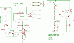
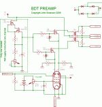
Have people seen John Swenson's new take on his BDT preamplifier http://www.audioasylum.com/cgi/vt.mpl?f=tubediy&m=141747
Apart from the unique use of Beam Deflection Tubes, there's an interesting twist on Gary Pimm's self bias CCS to make it into a Voltage regulator (par excellance, according to JS). This involves the addition of an error amplifier - full explanation is given on the thread referenced.
I'm wondering how this might be scaled up to higher currents for use in a tube output stage?
Is it a matter of using the Pentode configuration as per Gary Pimms explanation of higher current CCS & if so what other changes might be involved?
Attachments
jkeny said:I'm wondering how this might be scaled up to higher currents for use in a tube output stage?
Those output FET's are rated for 30W. Assuming you are regulating at a generous 50V below your supply input, Q2 would drop 90% of that - let's make it 45V. At 100mA output, you'd be dissipating 4.5W. With good heatsinking, you should be able to at least double that. You could probably parallel a couple of Q2, if you want a big safety margin.
Sheldon
Thanks Sheldon,
It seems it would be fine then in the current config - with heatsink on output Mosfets.?
I've been reading up on GP's Pentode version for higher currents in which he uses the pentode as an intelligent resistor to dissipate heat - plays no other role apparently! Can leave off the heatsink on Mosfet in that case.
If I was looking for a low voltage high current version say 40V/6A - I wonder would this circuit do the job?
Both LND150 and the IRF820 are 500V parts. If your input supply is never over about 450 with no load, you can regulate to 0V and not exceed part ratings. Input can be higher, but should not exceed output by more that 450V. A bigger margin will be better, say 400V in either case. If your input is higher than about 400V, go through the thought experiment to make sure that the voltage across any of the FET's will not exceed that during start up. Charging time of C2 should not be an issue if I've done the analysis correctly, but double check that.
Yes, I see no reason why you couldn't use this circuit for lower voltage higher current applications. In that case you'd need bigger FET's for the output. Input capacitance for the output FET will be an issue, especially since you'd probably want minimal voltage drop (look at the CRSS curves, vs ds voltage). So in that case you might substitute DN2540 or 10M45's for the LND150 and run about 10 or 20 mA through that string. Factor your resistors and capacitors accordingly. It looks like this circuit runs about 0.4mA, so for 16mA you'd need to decrease R1,2,3 by 40X and increase caps C1,2 by the same.
If you are thinking of doing it for the Zeus, it's overkill. PSRR is very good for that design. But hey, overkill is just enough here.
Sheldon
Edit: BTW, if you're planning to build the big Zeus, I've got a set of matched FET's, I'm probably not going to get to.
Ah, Sheldon, you remember me! The pack rat who got those lovely Lovoltech LU10140D from you but haven't done anything with them yet.
One of the issues holding me back was a preamp to drive the Zeus i.e. balanced & good drive.
But now this new BDT preamp comes at the right time & I'm looking to build it as the front end to a Zeus & a Baby Huey. I'll be building the "BIG" Zeus with FQA34N20 (these are replacement parts for the STW34NB20) Mosfets from which I matched two good pairs.
I believe this BDT will replace the Zeus input trafo & provide Vol control, gain & phase splitting making for a nice integrated amp.
I wasn't thinking about the low voltage regulator for the Zeus but for a Panasonic SAXR57 digital amp that uses Power Supply Voltage Control & needs a very good PS
I'll have to think about all you said as this doesn't come naturally to me!
Thanks again for your help - I'm sure I'll be leaning on you again if that's OK?
It's a nice little amp. I've only tried the JFET version. I played with a tube differential input stage, but it didn't offer any real advantage, other than higher input impedance compared to the transformer input. My source has an output impedance of 75R, so it's not really an issue, and I'm using it with the transformer now.
Sheldon
Sheldon
I have not had time to try John's regulator version of the CCS circuit yet. It looks like a very nice circuit. It should scale up nicely though.
Back when experimenting with filament CCS ideas one self bias CCS got loaded with FQPF50NO6L (60V 36A) MOSFETs with the cascode bias voltage dropped to just a few volts. Just to see what the circuit would take I kept increasing the current to see what would break first. Had to stop at 8 amps when the runs on the board started smoking! No part failures...
I gave up on the low voltage high current endeavors because they almost required running the MOSFETs at low voltage where the capacitance is high.
From experience gained from using the CCS circuit as an amplifier, the voltage across the lower MOSFET needs to be kept at 20 volts or higher for stability and performance issues. 20 volts is fine in circuits running up to the low hundreds of milliamps but not easy to do when talking about amps of current.
Thanks for chiming in Gary, and helping a couple of neophytes. My understanding is that the actual capacitance is not so much the issue as the fact that the slope of capacitance vs Vds is steep at low Vds. That's why I suggested a beefier fet for the bias side. Would this help enough? Sounds like your experience suggests that it would not. In principle, adequate current to the gate should overcome the problem (mostly, at least). If DN2540 were subbed for the LND150, the current could be raised even higher than the 10-20mA I proposed.
Sheldon
Sheldon
")
Thanks Gary & Sheldon,
It seems like the approach with Mosfets is not feasible - (in the datasheets for low ultra-low CRSS, it's impossible to make out the Crss at low voltages due to the scaling of the graphs)
How about bi-polars instead - what issues would this give rise to?
As you can tell I'm just a worker bee in this hive - thanks to both of you for your expertise & to Gary for this wonderfully versatile CCS.
It's amazing the number of different configurations this circuit has been transformed into
- Solid State Pentode amplifier
- I/V
- Transconductance amplifier
- Voltage Regulator
I'm probably missing a few?
Oh, BTW, has anybody done a run of Gary's boards yet? I'd be interested in buying some as I wired up the 250 V VR & the CCS on perfboard & it was a pain!
Actually, Sheldon,
I didn't fully pick up on your suggestion about substituting LND150 with DN2540 as a way out of the Mosfet over-heating issues! This would be worth investigating!
Could somebody on that side of the pond email me 10 or 20 of these that I would order from Mouser & I would order whatever number extra for that person to cover postage?
Please help a dummy in understanding this!
By increasing the current output of the LND150 voltage reference cascode (or substituted DN2540) drives more voltage into the gate of Q1 and this allows for a higher current output from the Mosfet - OK.
But how does this alleviate the problem of Drain to Source needing to be a voltage differential of 20V and at 8A causing Mosfet (circuit) overheating?
Still trying to learn the basics!
jkeny said:By increasing the current output of the LND150 voltage reference cascode (or substituted DN2540) drives more voltage into the gate of Q1 and this allows for a higher current output from the Mosfet - OK.
No. Current and voltage can be set independently. Current in the bias string is set by R1. The voltage across R2, sets the voltage difference between the gates (and outputs) of Q2 and Q1. This drop across R2 is, of course, set by the current delivered by the Q3/Q4 cascode. So if you decrease R1 to increase the current, you have to decrease R2 by the same proportion, to maintain the same voltage relationships as before.
The actual output voltage is set by the combined resistance of R3 and R8 (with Q5 to amplify the error detected at the output and feed back on the input) As for R2, this has to be calculated based on the current set by R1.
Voltage delivered to the gates of Q1 or Q2, has nothing to do with the current they can source. That depends entirely on the load and physical limitations of those FETs. Simplistically, if you need more current capacity, you use a bigger FET or parallel up a bunch of smaller ones (which is what bigger ones are anyway). The problem with that, is that you increase the capacitance seen at the gate. Further, the problem with that capacitance is not so much its absolute amount, it's that it increases rapidly as the voltage across the FET decreases toward zero (check out the curves for Crss - above about 20Vds, the capacitance becomes nearly constant). This changing capacitance means that the frequency response of the output will vary with voltage - not good for sound, as it's not something we would encounter naturally.
My suggestion of increasing the current through the bias string for high current applications was an attempt to provide enough current to push the frequency response issues high enough up in frequency to get any effects out of the audible range. Don't know if it is actually accomplished - that could be simulated. Gary suggests that it wasn't, but maybe he was using the LND150. That leaves the possibility that added bias current would help - maybe Gary will give help us here.
If more current still isn't enough, one could simply add enough capacitance across the gate, to swamp out the FET capacitance, and make the capacitance seen by the bias drivers essentially constant. Then, at least any roll off and it's consequent phase shift would be much more benign to the ear.
Sheldon
Ok, thanks for explaining Sheldon. I'm with you up to the second last paragraph
Sorry if all this is EE 101 but I'm still learning the basics!
The last suggestion of extra capacitance to swamp out the FET's seems too easy - there must be a downside to this?
I don't want to pester you but how does extra current do this? Are we not still operating in the CRSS area of high slope? Is the only way of operating in a more linear part of the graph through inreased voltage accross the FET?provide enough current to push the frequency response issues high enough up in frequency to get any effects out of the audible range
Sorry if all this is EE 101 but I'm still learning the basics!
The last suggestion of extra capacitance to swamp out the FET's seems too easy - there must be a downside to this?
jkeny said:how does extra current do this? Are we not still operating in the CRSS area of high slope? Is the only way of operating in a more linear part of the graph through inreased voltage accross the FET?
The last suggestion of extra capacitance to swamp out the FET's seems too easy - there must be a downside to this?
The issue is the impedance feeding the gate of Q1. I think in this circuit the impedance would be roughly equal to R2. And let's say we are using STW34NB20, a 200V, 34A rated FET. At 2Vds, Crss is about 1nF. Therefore the roll off corner (1/2piRC) would be at about 6kHz, and phase changes would start about a decade lower than that, at around 600Hz - clearly in the audio frequency range. If we want to decrease the impedance looking back from the gate by a factor of 20, we have to reduce R2 by that factor (1.35k). Well, Ohms law tells us, that in order to keep the voltage relationships the same, we need to pass 20 times the original current through it. That would get us to an f3 of 120kHz, and push up the start of phase changes to 12kHZ. Ok, now we are getting there.
If we increase the minimum voltage across Q1 to 5V then the Crss drops to about 300pF, push up the frequency changes by about 3 fold further.
Or, lets add 4nf from gate to source. Now, the corner drops 5 fold, from 120kHz to 24kHz, but the capacitance/Vds slope would be 1/5, or much shallower than before. The benefit is a flatter impedance/frequency response. The downside is the frequency response of supply is lowered overall.
How all this would affect the sound, I don't know - would depend to some degree on the amplifier PSRR. But I suspect that there would be some benefit to having your power supply frequency/phase constant at least up to the limit of the audio range.
Brian Beck describes the issue here: http://www.diyaudio.com/forums/showthread.php?postid=999010#post999010
Sheldon
One thing to note is that Brian, and I think Gary, are referring primarily to using the CCS in something like a plate load. In that case, the Vds changes with the signal. In the case of the regulated supply, the output voltage is constant, and the input to the control FET is also nearly constant, as it is isolated the the FET above it. Therefore, the slope of capacitance with Vds would not have as big an impact.
Maybe the main issue would be to make sure your power supply does not roll off lower than your amp. This could potentially cause problems of instability.
I think it's worth a try.
Sheldon
Maybe the main issue would be to make sure your power supply does not roll off lower than your amp. This could potentially cause problems of instability.
I think it's worth a try.
Sheldon
Thanks Sheldon,
So the absolute value of gate capacitance is the more important factor rather than the slope of change?
What I wanted to use this higher current/ low voltage reference for - a Panasonic SAXR57 Digital amp that uses voltage control to adjust the volume. It's range is from 10V to 40V at a max of 6A maybe. So this complicates matters I think & might make it not feasible given the gate capacitance rise at the lowest voltage
As the digital amp is a no feedback design, the quality of the PS is paramount (PSRR of zero).
I will probably give this a try after I've built up the BDT preamp & have learnt some more - thanks for your help in all this.
- Status
- This old topic is closed. If you want to reopen this topic, contact a moderator using the "Report Post" button.
- Home
- Amplifiers
- Tubes / Valves
- John Swenson's New BDT preamp