richwalters said:My guess that with that super Jfet and subsequent high speed driver (ideal), the high speed b/w stuff slows down with the b/w limitations of the output transformer. Instead of ss, I used RF tubes ECF80 and 12BY7 and had to stop down the response to avoid ringing in the output stage. In your design, be very interesting how square wave looks when completed.
richj
The open loop -3dB bandwidth of this part of the circuit is about 1MHz.
When the loop is closed, the open loop gain will need to be rolled off to maintain stability. This is what the RC pair labelled "comp" in the diagram is for.
I’ll have to figure out these values empirically once the whole thing is up and running.
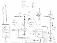
Here is the final circuit for the input amplifier bit. It's pretty simple, really.
A dual JFET input buffer followed by a LTP, followed by a cascoded high voltage LTP, followed by an emitter folower buffer. All HV transistors (2SC3417) are 70MHz fT CRT video amplifier devices with 1.8pF Cre.
Lag compensation is provided by R17 and C3 and the input LTP has a huge overload margin to amply cope with diminishing loop gain and a larger error signal at high frequencies. The feedback resistor and parallel lead compensation capacitor are mounted off board.
The circuit has a small signal bandwidth of about 1MHz, ensuring that it contributes negligible phase shift in its own right.
The source follower configured MOSFET’s used for the KT88 grid drive will be Fairchild FQP4N50 devices, which have a max Crss of 8pF. These will incur minimal phase shift driven from the emitter follower output. Loading will be by means of individual constant current sinks for negligible non-linearity.
Now onto the microcontroller board..........
An externally hosted image should be here but it was not working when we last tested it.
Here is a brief(ish) run down / some further details on how the microcontroller bias current system is going to be implemented for those who may be interested. A basic schematic diagram is attached below.
Time is limited, so I’ll just step through the relevant points in an unstylish manner that I hope will at least be coherent.
There are six KT88 valves in each channel, making 12 in total. Fix bias is used, with a quiescent/idle current (Ik) of approximately 55mA per KT88 (~330mA per channel) for class AB operation.
Each KT88 will require a fixed bias (grid one) voltage of about –75V. This bias voltage is derived from a regulated and stable –150V bias supply, a 100k series resistor and a programmable digital current sink, which is under the command of the PIC16F876A microcontroller.
Each KT88 has a one-ohm resistor in the cathode circuit for sensing the quiescent current. Since 55mA only incurs a voltage drop of 55mV across a one-ohm resistor, an ultra low offset instrumentation amplifier (50uV max) IC (INA118) is used to sense this voltage with minimal error. It is configured with a trimmable voltage gain of 50, thus producing an output voltage of 2.75V at Iq=55mA, which is fed directly into the 10-bit analogue-to-digital converter input of the PIC16F874A microcontroller.
A 12 way multiplexer, addressed by the microcontroller, selects one of the cathode-sensing resistors to measure at any one time. The microcontroller also has command over the HT power supplies and a input muting relay for each channel.
When power to the amplifier is first turned applied, the microcontroller will delay the application of HT to the KT88 plates for a time sufficient for the heaters to warm up (1 to 2 minutes I guess). The audio input of each channel will also be disabled by being re-routed to ground via the input relays.
During the warm-up interval, each of the twelve programmable current sinks will be preset to 0.00mA, thus applying the full –150V regulated bias voltage to each KT88 grid.
Once the warm up delay has elapsed, the HT will be activated and the full +500V applied to the KT88 plate circuit via the output-coupling transformer. At this time, the –150V grid bias applied to each tube ensures minimal cathode current.
The microcontroller will then systematically program each of the twelve KT88 bias currents in turn, ramping up the selected valves respective current sink until the 50mA bias current is reached. The microcontroller will alternately toggle between incrementing the programmable current sink and measuring the cathode current. (an array of flashing LED’s on the front panel will show what is going on).
Once the bias current to all twelve KT88’s is set, the microcontroller will disable the audio input mute applied to each channel, allowing the tunes to boom through.
Attachments
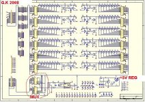
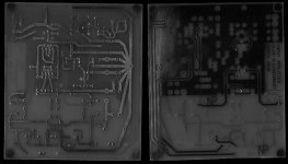
Below is a preview picture of the completed circuit for the measuring / biasing board. It contains the twelve digitally programmable current sinks, the 12 way multiplexer and the instrumentation amplifier.
The common data/control bus will connect to the microcontroller board via a 34-way ribbon cable.
Each current sink is comprised of a 74HC573 CMOS octal latch connected to a R/2R resistor ladder using 100k/200k resistors to form a 8-bit DAC. A simple opamp / MPSA92 PNP transistor circuit translates the current output of the R/2R ladder to a unipolar high voltage negative current sink.
A CMOS latch was used because its totem-pole MOSFET outputs swing right to the rails and have negligible output impedance WRT to the 200k/100k R/2R ladder, thus incurring very little error and making rather good performance / cheap DAC.
The only catch is that the translated output current from the R/2R ladder is a product of the supply voltage of the latch, which must therefore be stable and noise free.
This requirement is met by a +5V latch supply derived from the +15V supply with a LM336 voltage reference IC, buffered with an opamp and series pass Darlington transistor in its feedback loop.
A pair of 74HC4051 8-to-1 multiplexer IC form the 12 way multiplexer prior to the INA118 instrumentation amplifier IC.
The layout for this board is currently 50% complete, and is almost entirely layed out in SMD (to save having to hand drill the 400+ holes for the DAC resistors alone).
Attachments
G.Kleinschmidt said:The audio input of each channel will also be disabled by being re-routed to ground via the input relays. .
If I've got this right, you are shorting the inputs momentarily to ground during the warm-up duration. I did this on an amp and found the preamp output stage oscillating with near zero impedance. There is an issue of offset plops and thumps, when switching pre-amp off before the main amp is switched off.
richj
I built a similar microprocessor based auto bias system for a recent amplifier design. I blew up a couple of IC's before I figured out that the output tube can draw a lot more than the bias current on audio peaks, even more when it clips. There is always the possibility of a tube failure. I would add some series resistance between the 1 ohm resistor and the buffer chip with a 4.7 or 5.6 volt zener at the buffer input.
I see that you are pretty far along in the design cycle and may not want to change anything, but I found a simpler way to do the bias voltage. I use a SPI programmable dual D/A converter driven by the PIC chip. It drives a simple opamp - mosfet level shifter to make a zero to -150 volt programmable bias voltage. My implementation uses 6 chips to make 6 seperate bias circuits (3 dual D/A's and 4 dual opamps).
The design was done for a design contest sponsored by Microchip so I had to use their opamps which are all single supply 5 volt parts. I got better results with an opamp running on 12 volts since 5 volts barely turns on the mosfet.
The design is here. You can download the entire project entry. The circuit is well described in the entry text and the schematics are there, but hard to read. The schematics are also included in Eagle format. The bias generator is on page 2 of the controller schematic.
http://www.circuitcellar.com/microchip2007/winners/MT2209.html
richwalters said:
If I've got this right, you are shorting the inputs momentarily to ground during the warm-up duration. I did this on an amp and found the preamp output stage oscillating with near zero impedance. There is an issue of offset plops and thumps, when switching pre-amp off before the main amp is switched off.
richj
The input of the amp is shorted to ground and the preamp output is disconnected (SPDT relay for each channel)
Capacitive coupling on either side of the mute relay and resistive pull-downs to ground solve the thump and pop issue.
EDIT:
By audio input, I mean the actual input of the amplifier, not the RCA socket on the rear panel!
tubelab.com said:I built a similar microprocessor based auto bias system for a recent amplifier design. I blew up a couple of IC's before I figured out that the output tube can draw a lot more than the bias current on audio peaks, even more when it clips. There is always the possibility of a tube failure. I would add some series resistance between the 1 ohm resistor and the buffer chip with a 4.7 or 5.6 volt zener at the buffer input.
I see that you are pretty far along in the design cycle and may not want to change anything, but I found a simpler way to do the bias voltage. I use a SPI programmable dual D/A converter driven by the PIC chip. It drives a simple opamp - mosfet level shifter to make a zero to -150 volt programmable bias voltage. My implementation uses 6 chips to make 6 seperate bias circuits (3 dual D/A's and 4 dual opamps).
I did contemplate using IC DAC's, but not many come as dirt cheap as a bunch of 1206 resistors and some 74HC573's.
WRT to the level shifter, I have specifically gone the route of a programmable current sink instead of a programmable voltage source because of immunity to noise on and routing of the uC board and DAC board supply grounds.
WRT to dangerous voltages being developed across the cathode sense resistors, at 1ohm, a catode current of over 5A would be required to have any potential to zap the MUX. Not sure a KT88 could pass that from a +500V supply.
Cheers,
Glen
Not sure a KT88 could pass that from a +500V supply.
You are probably right. I was using 6336A's and 10 ohm resistors. I blasted a couple of mux chips before I added a series resistor and zener diodes.
I did contemplate using IC DAC's, but not many come as dirt cheap as a bunch of 1206 resistors and some 74HC573's.
This is true. I was bound by the rules of the design contest, and sprinkling in a few Microchip DACs and opamps was encouraged. Still, I would rather use a few $2 chips than a bunch of real cheap ones. It makes layout easier.
I have specifically gone the route of a programmable current sink instead of a programmable voltage source because of immunity to noise on and routing of the uC board and DAC board supply grounds.
You have a valid point here. I didn't notice any noise related issues with my design but my output stages are cathode followers. The drive requirements are huge. A few mV of noise directly on the grid of the output tubes would not be noticed. I did have LPF's on the amp board.
I put the controller (microprocessor, bias generator and agile SMPS) all on one board to satisfy the contest rules. When I build one for myself I will pay more attention to the construction and partitioning. Actually I plan to build three. Two SE designs (MicroTron, and MiniTron) and the monster that I described earlier, the Megatron. MiniTron is the contest amp with better software. The MicroTron is a little 8WPC SE amp using 7233's or Russian 6S19P's. No SMPS, and a mosfet is used to modulate the plate voltage on the output tubes. It is under currently construction. The Megatron will require a monster SMPS for the power supply (currently being developed) and another for plate voltage modulation.
tubelab.com said:You are probably right. I was using 6336A's and 10 ohm resistors. I blasted a couple of mux chips before I added a series resistor and zener diodes.
With 10 ohms, my MUX would fry at >0.5A. That would be possible with the KT88's. Though The reason I went for one ohm sense resistors is to eliminate their effect on the circuit.
The INA118 isn't exactly cheap, but is an elegant solution and I've got a few in my parts drawer.
tubelab.com said:This is true. I was bound by the rules of the design contest, and sprinkling in a few Microchip DACs and opamps was encouraged. Still, I would rather use a few $2 chips than a bunch of real cheap ones. It makes layout easier.[/B]
Well, I woudn't make my own DAC's for stuff I build for my employer (where it's a constant struggle for fit the required functionality into the given space) but for my own stuff, I like to play around. Little black blobs with SPI inputs are BORING!
tubelab.com said:You have a valid point here. I didn't notice any noise related issues with my design but my output stages are cathode followers. The drive requirements are huge. A few mV of noise directly on the grid of the output tubes would not be noticed. I did have LPF's on the amp board.[/B]
I think that either way, given enough attention to detail can be made to work and I'm sure that what you're got works perfectly well, but I'm building a BIG thingie here and anything that provides a little leeway with minimal extra complication WRT to bypassing and layout is a bonus.
Cheers,
Glen
G.Kleinschmidt said:I think that either way, given enough attention to detail can be made to work and I'm sure that what you're got works perfectly well, but I'm building a BIG thingie here and anything that provides a little leeway with minimal extra complication WRT to bypassing and layout is a bonus.
ARRGGHHH.
I ******** hate it when this POS Bill Gates software covertly fixes by typos with the substitution of incorrect words.

PS
Sorry for the rant.
EDIT:
....my typos....AARRGGGGGHHHHHHHHH!!!!!
Why use 6550s when TV tubes are so much better. My studio in Tracy enjoys over 400 watts of vacuum tube power; cost of the American nos glass was under $150. The massive cathodes on the sweep tube outputs have a knee current over an amp and it is a quad on each channel. Bass is as effortless as a solid state amp due to the huge current reserve and it's running McIntosh opt's so the power bw extends well past 100 kHz.
I am building one because I can, and it is different. I have breadboarded the typical push pull design using 6 X EH 6550. That is now "plan C". I got more power and punchier sound using 4 X 6LW6, now "plan B". Power output is in the 300 watt range.
The power supply is not too hard. The plate supply for the output tubes is a 480 volt to 120 volt 1 KVA industrial control transformer connected in reverse, feeding a SS bridge and CLC filtering. The choke is in the ground leg to avoid the need for a HV rated choke. Output is over 600 volts at 1 amp. Building a voltage regulator for this supply would be a serious experiment, but I am not convinced it is necessary.
I am currently experimenting with cathode follower output stages using 6LW6's or possibly 6336A's. This allows lower output impedance and distortion. I haven't got it all working right yet, so I may choose plan B or C at a later date.
I bought some Plitron toroidal OPT's that are rated for 400 watts at 20 Hz from their "surplus transformers" page last year for less money than the big Hammonds. Excellent transformers but the DC imbalance must be essentially zero, so I am using a microprocessor controller of my own design.
hey, tubelab, if 300 watts is your goal, then a pair of the QE08-200 gets you there....you need sockets for the 4-400 tube though....
https://frank.pocnet.net/sheets/030/q/QE08-200.pdf
hey, tubelab, if 300 watts is your goal
300 watts????? that was my goal eight years ago when I wrote that.....now, 500 watts, OK? Really my OPT's are rated for 400 watts at 20 Hz, so that should be the goal. The suggested tube set for this OPT is "six or eight 6550's."
then a pair of the QE08-200 gets you there
QE08-200's are pretty rare and expensive in the USA, It takes 750 volts B+ and 3600 ohms to get 300 W. Not a good match for my OPT's. I am looking at using parts and tubes that I already have.
Why use 6550s when TV tubes are so much better.
Gee, why didn't I say that......OH, wait a minute, I have been saying that for a while.....
The suggestion of 6 or 8 6550's and the 1250 ohm impedance implies a B+ voltage in the 600 to 650 volt range, so with those limitations, I can think of several ways to get there.....All involve TV sweep tubes. 4 or 6 X 6LW6's, 8 X 6HJ5's, 6 X 35LR6's, 10 X 13GB5's........
Many things changed or delayed my plans years ago. I have since "retired" (been laid off) and moved 1200 miles. I am in the process of building my new lab, but as you know I have already seen 250 watts flow from some transmitting tubes......more to come.
I have picked up where I left off about 5 years ago, where I saw 525 watts flow from 4 X 35LR6's using the same OPT's that I plan to use when the "big one" finally gets built.
I have designed a new driver circuit and I am currently working with 13GB5's and other expendable parts to iron out the kinks and optimize the design......which is straight G1 drive for now. Next, a 125 WPC amp gets built with Edcor iron, then the biggie!
Crazy drive and screen drive are too unconventional and still relatively unpredictable for a 500 WPC amp.
- Status
- This old topic is closed. If you want to reopen this topic, contact a moderator using the "Report Post" button.
- Home
- Amplifiers
- Tubes / Valves
- Hammond 1650W