Hey all, Don here over from the guitar tube amp world. I have built a number of amps using turrets and eyelets and want to now try out PCB. It has worked well for my power supplies and switching boards, now I am faced with the preamp and PI. I am looking for suggestions on PCB design tips for tube amps.
Here is what I have collected so far:
- use double sided, with plated through holes
- keep low impedance lines away from high impedance ones
- signal on one side of the board, power and ground on the other
- avoid parallel traces - either on the same side or opposite sides
- if lines cross (either side of the board) try to cross at 90 degrees
Any other suggestions? What about heater traces? Also not so sure about how to design with ground planes - won't this create a lot of capacitance?
Perhaps any web sites or books on this?
thanks!
Hey all thanks for the replies.
Geek, I am on the island so a little far away for coffee, alas. I would love to check out your shop and vice versa. Do you do your PCBs in your shop or farm it out? I would love to find thick double sided board that has photo resist on it for my at home prototypes. I currently use MG chemicals boards - a little lightweight.
Blisterfingers, I just ordered that book! I am looking forward to reading it.
Psychobiker, I thought autorouters were a no-no in the tube amp world. Regardless I 'll will investigate.
thanks!.
Hi,
Well, we'll have to meet you on the Island at Planet10's summer diyAudio festival or something")
Import most of them ready made.
Cheers!
Well, we'll have to meet you on the Island at Planet10's summer diyAudio festival or something
d1camero said:Do you do your PCBs in your shop or farm it out?
Import most of them ready made.
Cheers!
Hey all you tube/PCB experts, I am starting to design a double sided board and I m wondering about the layers. What is best?
- signal on bottom side
- power and switch signals on top side
where to put the ground - should it be a ground plane?
This is a preamp board with a few 9 pin sockets on it.
thanks
Don
- signal on bottom side
- power and switch signals on top side
where to put the ground - should it be a ground plane?
This is a preamp board with a few 9 pin sockets on it.
thanks
Don
There are design rules for trace width and how thick, oz. of copper...depending on the current density..
I have designed boards that handle 30 Amps for reliable flight operations.....so the heaters for tubes should not be a problem if done correctly...
Ground plane is the only way to go....
Stay away from vias in audio path.....
Chris
I have designed boards that handle 30 Amps for reliable flight operations.....so the heaters for tubes should not be a problem if done correctly...
Ground plane is the only way to go....
Stay away from vias in audio path.....
Chris
In re-reading my note, obviously I was a touch mess up. My question, better put is here:
I am using a two-sided board. What sides do I put the B+, signal and ground plane on?
So far, the signal is on the bottom side, and the B+ is on the top. I am not sure which side to put the ground.
thanks
I am using a two-sided board. What sides do I put the B+, signal and ground plane on?
So far, the signal is on the bottom side, and the B+ is on the top. I am not sure which side to put the ground.
thanks
d1camero said:
So far, the signal is on the bottom side, and the B+ is on the top. I am not sure which side to put the ground.
thanks
I did just such a design and after a year's use so much dust had accumulated around the B+ tracks (500V) which was making noises with ajacent tracks so I did a redesign and put both ground and signal on the underneath and B+ above and varnished the tracks. It does imply some complication routing but is worth it.
Where power components are mounted on fiberglass, I drilled air circulation holes directly underneath.
Where there is heat and some airflow, static dust accumulates around B+ tracks. A hint is to see how much dust settles around the EHT sections of a TV !
Ultimately the tag strips method is by far the best.
Major telecoms and computer designs often use 5V at 60A + with multilayer. Even with 2 sided, provided tracks are thick enough perhaps with extra strip Cu soldered....can't see any problem with heater currents..
richj
Rich thanks for the detailed reply. I will follow your advice!
As for heaters, it is not the current it is trying to keep AC hum out of the signal path. One recommendation was to wire the heaters in separate with twisted pair. Ths is how one builder did it for AX84 Firefly guitar amp.
I did have heaters on one board, but a lot of hum got through. Not sure how much was the board as I was dealing with grounding issues at the time as well - poor grounding scheme can cause lots of hum to creep in.
One further question: do you suggest that the ground be a ground plane or should I follow my "tried-and-true" star ground method that I have on my hand wired amps?
Don
These are just personal observations as I'm sure some people have had good results doing otherwise.
I've tried the ground plane method a few times, but the performance was never better than the star and buss grounding for Class A circuits. Sometimes it seems better for the current to return to one point before another as it does in star and buss grounding. Ground plane is defiantly a safer solution for someone inexperienced with other grounding methods. But if you are experienced with other methods stick to the tried and true.
Putting signal and power on the same side of the board has never been a problem as long as clearances are generous.
As Cerrem mentioned, keep vias out of the signal path. In fact, it would be best to keep vias out completely if possible. The power supply is part of the signal path too.
AC heaters would be best kept off the board, but DC heaters are no biggie if put on the board.
Place grid stoppers as close to the socket pin as possible.
Jeb-D. said:
Place grid stoppers as close to the socket pin as possible.
Worth a mention. I knew someone who built a tube amp with alot of SMD stuff in it, and soon after I was the one who repaired it. Tempting it is to use Melf resistors and caps, (if one can get 'em cheap enough) make sure the PCB is mechanically evenly fixed, i.e can screw down with distorting it and components.
The damage is obvious and can easily happen when a tube is withdrawn from socket and stresses the PCB.
I go along with Jeb-D regarding grounding impedance. With point to point wiring doing a stereo amp, keep symmetrical earth layout and circuit amp earth bus to chassis near input tubes. Avoid using the input socket for earth. It is poor. Better is a thick LoZ Cu strip to chassis close by.
Same applies to PCD except as copper plane.
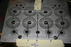
With PCB layout have a massive earth track plane and keep layout symmetrical where poss, esp relative to mains and psu chokes..(this will reduce eddy currents set up around pcb) This won't be quite as easy. I always try and engineer for the worst case that is one might have to find a " compromise sweet spot" common to each stereo half near input circuitry.Shown as arrows with enclosed photo. The PSU ground is done at the other end.With an AC heater supply, the old remedy of using a 100R 3W pot wired across the heater with wiper to chassis can often solve problems.
richj
Attachments
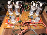
I do single side toner transfer, etched in ziploc bag, eyelets for wire connections and feedthroughts to mount caps to the copper side.
I jump to top side for all; B+, signal and ground. The back side is mostly ground plane. If going 2 layer the top would also be ground plane.
I always run the heaters as a twisted pair 3/4" from the back side. and on some, dual heater or triple heaters wire sets are used for 17V, 5V and 6.3V.
It will take me around 4 to 6hrs to get a PCB ready to drill and assemble/install the eyelets. I would like to have a real PCB double sided with heavy plated feedthroughs instead, but that takes longer and co$ts much more.
Attachments
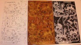
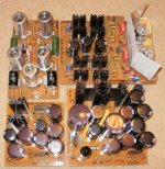
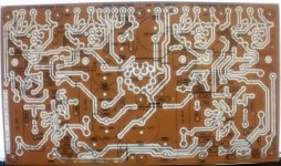
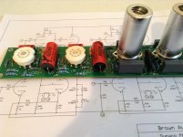
some more examples... the PCB on the left was stuffed and is the last couple of pics above.
The design was altered to add a power Zener-mosfet in place of a resistor and some of the traces were increased in width. When I use PCB express software I can design for toner transfer or real PCB design which are not the same artwork. For toner transfer I print a combo of top and back for the single back side. I use yellow silkscreen to show where the jumpers go on the top side.
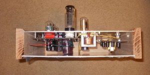
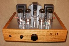
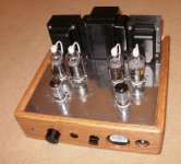
A side shot of the Keg-ear amp, the Keg-ear PCB and finished amp. ( 6L6-Kt88 family) The last pic is one of the earlier 6GV5 sweep tubes from the first couple of pics above.
and what they can turn into at the end......
The design was altered to add a power Zener-mosfet in place of a resistor and some of the traces were increased in width. When I use PCB express software I can design for toner transfer or real PCB design which are not the same artwork. For toner transfer I print a combo of top and back for the single back side. I use yellow silkscreen to show where the jumpers go on the top side.
A side shot of the Keg-ear amp, the Keg-ear PCB and finished amp. ( 6L6-Kt88 family) The last pic is one of the earlier 6GV5 sweep tubes from the first couple of pics above.
and what they can turn into at the end......
Attachments
Last edited:
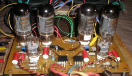
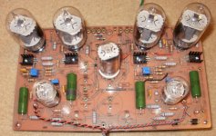
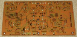
Really good recommendations so far. I have an example of a current project consisting of a phono stage and line stage preamp. You will notice the narrow layout, to accommodate a low profile enclosure. I'm using DC on the heaters,and for that I'm able to run the traces on board to minimize noise,and wiring. I've been using ExpressPCB for 2 or 3 years, they are a little pricy, but they are consistent on quality and turn around.
Attachments
Last edited:
It will take me around 4 to 6hrs to get a PCB ready to drill and assemble/install the eyelets. I would like to have a real PCB double sided with heavy plated feedthroughs instead, but that takes longer and co$ts much more.
I noticed the use of eyelets. (Great photos, and some really good boards too.)
Have you seen any problems caused by differential thermal expansion between the eyelet and the rest of the PCB? I remember seeing boards using this technique back in the 70's and after a few years they would start yo get a few hairline fractures at some of the though PCB connections. They eyelets used then were probably different and the solder would have been regular tin-lead of course.
When I was involved with aerospace electronics at TRW ( TDRSS, IUS, Shuttle), the main problem that we experienced was the thermal fatigue caused by not having the proper lead form on components to allow for thermal expansion. We also had a few failures on 8 layer PCBs with the plated through holes developing cracks in the barrels causing disconnects between the layers. This was improved by allowing the through holes to be a little larger in size and thus allowing the solder to wick from bottom to top during wave soldering. The only issue with the eyelets has been not soldering them to the traces, mechanical flaring only and developing intermittent connections... I solder all eyelets to the traces and no problems.
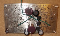
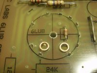
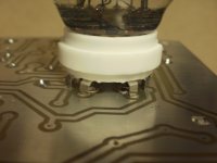
The 6LU8 amp was done with the PCB designed upside down, traces to the top and components on the bottom. After the tube sockets were installed the leads were bent over for mechanical security and then the leads were soldered to the traces. The leads must be firmly bent over to prevent from pulling the traces off the PCB. Double sided PCB's solve this issue.
The 6LU8 amp was done with the PCB designed upside down, traces to the top and components on the bottom. After the tube sockets were installed the leads were bent over for mechanical security and then the leads were soldered to the traces. The leads must be firmly bent over to prevent from pulling the traces off the PCB. Double sided PCB's solve this issue.
Attachments
- Status
- This old topic is closed. If you want to reopen this topic, contact a moderator using the "Report Post" button.
- Home
- Amplifiers
- Tubes / Valves
- PCB design techniques for Tube Amps