I think YBA did one as well, 25 years ago. Makes most bipolar amps very prone to thermal runaway. Personally, I like emitter resistors, IF they are good quality, and small enough to be 'optimum' in value. They thermally stabilize the output stage, and help balance parallel device currents.
What is ironic is that Charles Hansen, Parasound and I, as well as perhaps several other designers here, have ALL these parts and have used them for decades, and continue to do so today, however, with some care, and difficulty in getting discontinued devices. It is true that they have gotten more expensive. WELL, so what? Constantly looking for a bargain might be 'fun' for some people, but I find it a waste of time, UNLESS I come across one in my work, and then I grab it for the future. That gives me a prudent reserve.
There is a 'history' of jfets that is a little irregular. The original method of making jfets could produce very quiet devices on occasion and sometimes, some very noisy ones. Luck of the draw, or the batch. Later, many manufacturers switched to 'ion implantation' including Toshiba, and that is when really bad things started to happen. Apparently, the process is cheaper, but cruder. The use of these devices as SWITCHES was not fundamentally effected by this added low frequency noise, but audio sure suffered. However, Toshiba generally recovered from their original problems and made pretty good parts up to the present day, but now they are ceasing production.
Linear Systems will soon 'take up the slack' so to speak, BUT they will NOT be the $.19 parts any more, and will be in the several dollar range for premium parts. But so what, if you are an amateur? It is a one time cost, and look at the results! It is a bit like Solder. I use solder that is fairly expensive, SN62. Why? Because it FLOWS BETTER and gives me less chance of making a 'cold joint' (I used to make a lot of them in the old days), AND I think it IS a better solder connection than SN60. My cost, maybe $50 every 2 years. Big deal!
The history of the Siliconix J272, P channel device is also long and somewhat varied.
First used in the Levinson JC-2, starting in 1973, the device was fairly quiet, but prone to some 1/f noise. I chose NOT to use it for a phono input at the time, because of this. Later, National second sourced this part, AND somewhere along the line, we had some distortion problems with some of these devices, probably because of Ion implantation being tried and used, and this was back in the 1970's. By 1976, Siliconix completely ruined the J110, a very low noise N channel part, for several years, by switching to ion implantation, YET they did NOT change the noise graph for the device in the data book.
This is a potential headache, that we have to avoid, i.e. trusting manufacturer's graphs, without double checking, ourselves.
What Scott is warning about with the Fairchild J271's is that they MIGHT be very noisy, due to ion implant processing or whatever. They too, would have to be tested, but if a distributor had a good batch, then ordering more would be a wonderful opportunity for someone to get them cheap and easy. If they are noisy, then you have an extra $20 worth of parts in a small plastic bag that you can use for prototypes and line stages. But, you have to try, and not just 'whine' about the situation.
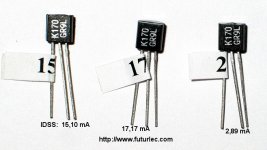
This is a bit off topic, but earlier in the thread there was mention of fake Toshiba JFETs on ebay and others have mentioned this on the forum. How do you tell a fake? Is the Idss way off? Or is it hard to tell?
I know someone who bought a whole bunch on ebay awhile back ... not me, almost me.
I know someone who bought a whole bunch on ebay awhile back ... not me, almost me.
JC said:Linear Systems will soon 'take up the slack' so to speak, BUT they will NOT be the $.19 parts any more, and will be in the several dollar range for premium parts. But so what, if you are an amateur? It is a one time cost, and look at the results!
I used the LSK170Cs in a preamp design and couldn't be happier with it.
Any input on the Technical Brain amplifiers? They claim their highly praised amps are the result of eliminating the emitter resistors. A supposed completely new design approach.
Dartzeel also.
It does appear to change the sound, but some of the implementations have
not been very reliable for obvious reasons.

YBA did one
Not in the earlier products, afair, the L'Integré from 1987 has emitter resistors.
As did Mr André's first power amp model YBA1 from 1990, plus the later YBA 1HC, YBA2, YBA 2HC.
Toshiba's 2SJ73/2SK146 600mW duallies cost $6 each at local shops overhere +20 years ago (pre Desert Storm exchange rate).
Makes $3 per JFET, to have a pair of tight Idss matched duallies required buying at least 10, ordering by the 100(s) made them a lot cheaper.
+$2 each average for a 400mW P/N-channel still is silly money in pre-1990 value.
(not that i've ever paid 2 bucks for a single JFET, but give me time
 )
)
Last edited:
This is a bit off topic, but earlier in the thread there was mention of fake Toshiba JFETs on ebay and others have mentioned this on the forum. How do you tell a fake? Is the Idss way off? Or is it hard to tell?
I know someone who bought a whole bunch on ebay awhile back ... not me, almost me.
FYI, If anyone has suspected fakes I might be able to sneak some into the QC lab to have the plastic removed. I was thinking of doing some real ones in any case (just have to lie a little
).Stop worrying and just do it.Dont do that, I for one am very grateful that there are many professionals on this board, but lately I have been thinking about how much kit I would need to buy to do all of these things to match devices etc. Measuring the i/f noise seemed to be one of those that take a lot of effort and £/$. then I glanced up at the URL bar and it struck me me are drifting away from the original aim of this board. We do it because we are engineers and curious enough to keep improving the mousetrap so to speak.
Wrinkle
Yawn...we did it 18 years ago:
http://www.diyaudio.com/forums/soli...ilt-non-feedback-amplifier-24.html#post334963
I'm sure there are others as well.
Amazing how folks obsess when the extrinsic internal resistances are made out of "horrible" stuff.
Later, many manufacturers switched to 'ion implantation' including Toshiba, and that is when really bad things started to happen. Apparently, the process is cheaper, but cruder.
John this is a statement made from complete ignorance of what goes on in the IC industry. Nothing could be further from the truth, ion implantation was developed to tightly control doping profiles in modern processes.
FYI, If anyone has suspected fakes I might be able to sneak some into the QC lab to have the plastic removed. I was thinking of doing some real ones in any case (just have to lie a little
Scott,
I bought a few "2SJ74bl" on ebay from a HK seller which seem to be fakes. Their Idss is way out of range on the high side. Not surprisingly, the seller's account was suspended not long after I bought them.
I'd be glad to send a few your way if you want to see what's inside.
---Gary
Scott,
I bought a few "2SJ74bl" on ebay from a HK seller which seem to be fakes. Their Idss is way out of range on the high side. Not surprisingly, the seller's account was suspended not long after I bought them.
I'd be glad to send a few your way if you want to see what's inside.
---Gary
Sounds like rebrands of those huge Idss switching FET's, I'll PM you from work.
I just spoke with Kirkwood Rough. He says that ION IMPLANTATION is very problematic, and if done wrong, (and often is) WILL cause noise. He also says that MASK ALIGNMENT is a serious problem as well. He designs jfets for a living, being a consultant for Linear Systems with jfet design.
You guys have nailed the issue. It isn't "bargain hunting." If you're making commercial stuff, great, you find some real ones and stock up with what you'll need for forseeable production runs. Advanced experimenters can buy a few here and there, then check them to see if they're real. For those of us trying to publish designs for others to build, parts have to be reliably obtainable. I've had a couple people I trust offer to get a pile of real ones for me, but that doesn't solve the issue for anyone who would want to diy (that's what this site is about!) from plans. The last thing I want to do is get involved with group buys or do anything even vaguely commercial in audio.
Besically, pFETs with low noise are just not realistic for diy designs until LS gets into that business- or unless someone else wants to do a group buy.
Besically, pFETs with low noise are just not realistic for diy designs until LS gets into that business- or unless someone else wants to do a group buy.
This is a bit off topic, but earlier in the thread there was mention of fake Toshiba JFETs on ebay and others have mentioned this on the forum. How do you tell a fake? Is the Idss way off? Or is it hard to tell?
Letters are stamped with silver ink, not engraved. they can be easy erased with alcohol or acetone. And Idss is usually way off.
Attachments
I just spoke with Kirkwood Rough. He says that ION IMPLANTATION is very problematic, and if done wrong, (and often is) WILL cause noise. He also says that MASK ALIGNMENT is a serious problem as well. He designs jfets for a living, being a consultant for Linear Systems with jfet design.
John,
I think the information that you're passing along from Kirkwood is a bit simplistic. I'm sure that he knows the details but reducing the issue to Ion Implantation and Mask Alignment is not very helpful to the general reader. In an earlier part of my career, I developed process technology for very high volume manufacturing. Based on that experience, here's what I think is going on.
Typically, the source of noise in silicon devices is related to defect traps at the interface between the silicon and the insulator. The insulator is typical SiO2 (silicon dioxide). Many, many years ago, the n+ and p+ junctions for transistors were made by diffusing dopants at very high temperatures - arsenic (As) or phosphorus (P) for n+ junctions and boron (B) for p+ junctions. As people tried to scale devices to smaller dimensions, they needed to make the junctions shallower so that the would move a lesser amount laterally. This became hard to do with diffused junctions and people moved to ion implantation where one ionizes a dopant and then accelerates the ions into the silicon so that they are deposited below the silicon surface. This allows one to count the exact number of dopant atoms put into the silicon. Ion implantation creates some damage which needs to be annealed out. If the damage isn't properly annealed then this can lead to excess junction leakage and also excess noise. It's easy to measure junction leakage and this is often the thing used to optimize the annealing conditions. Removing the damage that causes junction leakage doesn't necessarily remove the damage that causes excess noise. One is related to defects in the silicon while the other is related to defects at the Si/SiO2 interface. Obviously both types of damage can be removed, since Toshiba learned to do it. So it's not fundamental - it's just means manufacturers have to relearn the tricks that others have already figured out.
---Gary
Letters are stamped with silver ink, not engraved. they can be easy erased with alcohol or acetone. And Idss is usually way off.
Thanks, I'll let my friend know.
Just a quick post about fake/genuine Toshiba fets. If anyone wants to pursue this in more detail there is a v.helpful thread started last month. Called "2SK170BL and 2SJ74BL" by Russellc on the 6th May this year. It has a lot of info' including photos of fake/genuine parts, written descriptions of characteristics and anecdotal experience form purchasers.
Hobbyists might find this thread useful...
Hobbyists might find this thread useful...
- Status
- Not open for further replies.
- Home
- Member Areas
- The Lounge
- John Curl's Blowtorch preamplifier part II